Hi,
I'm not familiar with PSPICE for TI. I've tried to simulate a SEPIC converter using the LM3488 device.
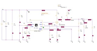
I've attached the schematic and the out file from the simulation.
Could I get pointed in the right direction to find help for debugging these PSpice simulation errors or help me directly with debugging my simulation?
I've been searching the e2e forums and I can't figure out what is preventing the sim from running.
**** 07/12/23 15:58:52 ******* PSpice 17.4.0 (Nov 2018) ******* ID# 0 ********

 ** Profile: "SCHEMATIC1-Steady State"  [ G:\Engineering\Simulations\lm3488-pspi


 ****     CIRCUIT DESCRIPTION


******************************************************************************


** Creating circuit file "Steady State.cir"
** WARNING: THIS AUTOMATICALLY GENERATED FILE MAY BE OVERWRITTEN BY SUBSEQUENT SIMULATIONS

*Libraries:
* Profile Libraries :
* Local Libraries :
* From [PSPICE NETLIST] section of C:\cds_spb_home\cdssetup\OrCAD_PSpiceTIPSpice_Install\17.4.0\PSpice.ini file:
.lib "nom_pspti.lib"
.lib "nom.lib"

*Analysis directives:
.TRAN  0 80u 0 0.01u
.OPTIONS ADVCONV
.OPTIONS FILEMODELSEARCH
.PROBE64 V(alias(*)) I(alias(*)) W(alias(*)) D(alias(*)) NOISE(alias(*))
.INC "..\SCHEMATIC1.net"


**** INCLUDING SCHEMATIC1.net ****
* source LM3488-SIM
X_U1         0 N01866 N01439 N01821 N01523 N01326 0 VIN LM3488_TRANS PARAMS:
+  SS={SS}
X_U2         N01458 N01439 N01387 CSD19538Q3A
L_L1         N01458 VIN  33u
L_L2         N01467 0  33u
C_C4         VIN 0  10u
C_C5         0 VIN  0.1u  TC=0,0
C_C6         0 N01866  510p  TC=0,0
C_C7         0 N01901  0.1u  TC=0,0
R_R1         N01901 N01866  1.3k TC=0,0
R_R2         0 N01821  31.6k TC=0,0
R_R3         0 VIN  10k TC=0,0
C_C8         N01467 N01458  1u  TC=0,0
C_C9         VOUT 0  47u IC={11.5*SS}
R_R4         VOUT N01523  84.5k TC=0,0
R_R5         N01523 0  10k TC=0,0
R_R6         N01387 0  0.05 TC=0,0
R_R7         N01326 N01387  100 TC=0,0
C_C10         0 N01326  680p  TC=0,0
V_V1         VIN 0 12Vdc
D_D1         N01467 VOUT Dbreak
R_R8         VOUT 0  1 TC=0,0
Kn_K1         L_L1 L_L2     1
.PARAM  ss=1

**** RESUMING "Steady State.cir" ****
.END

INFO(ORPSIM-15453): Model X_U2.NMOS: Using BSIM VERSION 3.2

**** 07/12/23 15:58:52 ******* PSpice 17.4.0 (Nov 2018) ******* ID# 0 ********

 ** Profile: "SCHEMATIC1-Steady State"  [ G:\Engineering\Simulations\lm3488-pspi


 ****     Diode MODEL PARAMETERS


******************************************************************************


               X_U2.DBD
  T_Measured   25
   T_Current   27
          IS  500.000000E-15
           N    1.06
          BV  101
          RS    4.000000E-03
          TT    2.000000E-09
         CJO    7.500000E-15
          VJ     .5
           M     .625
         XTI    3.3
        TRS1    4.000000E-03


**** 07/12/23 15:58:52 ******* PSpice 17.4.0 (Nov 2018) ******* ID# 0 ********

 ** Profile: "SCHEMATIC1-Steady State"  [ G:\Engineering\Simulations\lm3488-pspi


 ****     MOSFET MODEL PARAMETERS


******************************************************************************


               X_U2.NMOS       X_U2.PMOSd
               NMOS            PMOS
  T_Measured   25              27
   T_Current   27              27
       LEVEL    7               1
           L  100.000000E-06  100.000000E-06
           W  100.000000E-06  100.000000E-06
         VTO     .7             -.3
          KP   51.797160E-06   51.797160E-06
       GAMMA    0              10
         PHI                     .954626
      LAMBDA    0               0
          IS    1.000000E-15   60.000000E-15
          JS    0               0
          PB    1                .8
        PBSW    1                .8
          CJ    1.000000E-18    1.000000E-18
        CJSW    1.000000E-18    1.000000E-18
        CGSO    1.000000E-18    1.000000E-18
        CGDO    1.000000E-18    1.000000E-18
        CGBO    1.000000E-18    0
        NSUB   10.000000E+15    1.500000E+18
         TOX   40.000000E-09   40.000000E-09
          XJ  300.000000E-09    0
       UCRIT   10.000000E+03   10.000000E+03
       DELTA     .022
      DIOMOD    2               1
         VFB   -1               0
        LETA    0               0
        WETA    0               0
          U0  600               0
        TEMP                    0
         VDD                    5
       XPART    0               0
          UA   14.000000E-09
          UB    5.000000E-18
          UC  -46.500000E-12
        VSAT   80.000000E+03
        RDSW    0
        VOFF     .1
     NFACTOR    2
        PCLM     .25
      PDIBL1     .02
      PDIBL2    4.000000E-03
       DROUT     .9
      PSCBE1  300.000000E+06
      PSCBE2    1.000000E-06
          A0    1
          A1    0
          A2    1
       NPEAK  148.500000E+15
         VBM   -5
         LDD    0
        LITL  189.736700E-09
         KT1   -1.15
         UA1   25.000000E-12
         UB1 -800.000000E-21
         UC1  -56.000000E-12
        PVAG     .1
        ETA0    5.000000E-03
        KT1L    1.000000E-15
        DSUB    1.4
      MOBMOD    1
        PRWG    0
        LINT   55.000000E-09
         DLC   55.000000E-09
         DWC    0
          CF    0
        NOIA  100.000000E+18
        NOIB   50.000000E+03
        NOIC   -1.400000E-12
         VTM     .025692
     VERSION    3.2
       PBSWG    1
       MJSWG     .33
       CJSWG    1.000000E-18
       JTSCD    0
        TOXM   40.000000E-09
         LLC    0
         LWC    0
        LWLC    0
         WLC    0
         WWC    0
        WWLC    0


**** 07/12/23 15:58:52 ******* PSpice 17.4.0 (Nov 2018) ******* ID# 0 ********

 ** Profile: "SCHEMATIC1-Steady State"  [ G:\Engineering\Simulations\lm3488-pspi


 ****     Resistor MODEL PARAMETERS


******************************************************************************


               X_U2.RTEMP
           R    1
         TC1    6.000000E-03
         TC2   20.000000E-06


**** 07/12/23 15:58:52 ******* PSpice 17.4.0 (Nov 2018) ******* ID# 0 ********

 ** Profile: "SCHEMATIC1-Steady State"  [ G:\Engineering\Simulations\lm3488-pspi


 ****     INITIAL TRANSIENT SOLUTION       TEMPERATURE =   27.000 DEG C


******************************************************************************


 NODE   VOLTAGE     NODE   VOLTAGE     NODE   VOLTAGE     NODE   VOLTAGE


(  VIN)   12.0000  ( VOUT)   11.4770  (N01326)-625.9E-06 (N01387)-312.8E-09

(N01439) 28.79E-12 (N01458)   12.0000 (N01467)-855.5E-18 (N01523)    1.2145

(N01821)     .9693 (N01866)    1.6929 (N01901)    1.6929 (X_U2.4)   12.0000

(X_U2.5) 28.79E-12 (X_U2.6)-312.8E-09 (X_U2.7)   12.0000 (X_U2.8)-312.8E-09

(X_U2.9)-312.8E-09 (X_U1.FA)     .9693                   (X_U1.OC)    0.0000

(X_U1.OV)    0.0000                   (X_U1.SS) 1.701E-06

(X_U2.10)   12.0000                   (X_U2.11) 28.79E-12

(X_U2.12)-312.8E-09                   (X_U1.CLK)     .2000

(X_U1.OC1)    0.0000                  (X_U1.OC2)    0.0000

(X_U1.REF) 1.701E-06                  (X_U1.SET)    0.0000

(X_U1.VCC)    7.1811                  (X_U1.RAMP)    -.0625

(X_U1.UVLO)    2.5000                 (X_U1.V7P2)    7.1811

(X_U1.FBVAL)    1.2145                (X_U1.OCDLY)    0.0000

(X_U1.RESET)    1.0000                (X_U1.X_U2.3)    0.0000

(X_U1.X_U2.5) 24.38E-06               (X_U1.X_U7.1)    1.0000

(X_U2.xcds.5)   12.0000               (X_U2.xcds.6) 94.50E-12

(X_U2.xcds.7)    0.0000               (X_U2.xcds.8)    0.0000

(X_U2.xcgd.5)   12.0000               (X_U2.xcgd.6) 11.40E-12

(X_U2.xcgd.7)    0.0000               (X_U2.xcgd.8)    0.0000

(X_U1.DRVRSIG)   -3.0000              (X_U1.OSCSHUT)    0.0000

(X_U1.PWM_CLK)    0.0000              (X_U1.VGM_REF)    1.2600

(X_U1.X_U2.12)    0.0000              (X_U1.X_U2.13)     .0619

(X_U1.COMP_NEG)     .3589             (X_U1.COMP_POS)-625.9E-06

(X_U1.X_U2.FSW) 476.0E+03             (X_U1.N16850239)    0.0000

(X_U1.N16855996)   -3.0000            (X_U1.N16875644)    1.0000

(X_U1.N16907101)    0.0000            (X_U1.N16908277)    1.0000

(X_U1.N16909753)    1.0000            (X_U1.N16926804)    2.8500

(X_U1.N16927149)     .1700            (X_U1.N16930285)    1.0000

(X_U1.N16931482)    1.0000            (X_U1.N16943331)    2.8000

(X_U1.N16943348)    2.3820            (X_U1.N16945907)    0.0000

(X_U1.N16966720)    1.0000            (X_U1.X_U10.MY5)    1.0000

(X_U1.X_U10.Qbr)    1.0000            (X_U1.X_U10.Qqq) 2.002E-15

(X_U1.X_U2.0P1V)    0.0000            (X_U1.X_U3.YINT)    1.0000

(X_U1.X_U5.YINT)    1.0000            (X_U1.X_U6.YINT)    1.0000

(X_U1.X_U7.INM1)   -9.1500            (X_U1.X_U7.INP1)    0.0000

(X_U1.X_U7.INP2)     .1700            (X_U1.FB_NOSPIKE)    1.2145

(X_U1.X_erramp.1)    1.4108           (X_U1.X_erramp.2)     .0455

(X_U1.X_erramp.3)    1.4108           (X_U1.X_erramp.4)    1.4108

(X_U1.X_erramp.5)    1.4108           (X_U1.X_erramp.9)    1.4108

(X_U1.X_U10.Qint) 2.002E-15           (X_U1.X_U2.FABY5)    0.0000

(X_U1.X_U2.FAINT)     .9693           (X_U1.X_erramp.10)    5.0000

(X_U1.X_erramp.11)    1.3000          (X_U1.X_U1.TONMIN)    0.0000

(X_U1.X_U10.MYVSS)    0.0000          (X_U1.X_U10.Qqqd1)    0.0000

(X_U1.X_U137.YINT)    0.0000          (X_U1.X_U2.FA_GEN)    1.0000

(X_U1.X_U2.VCO_SQ)    0.0000          (X_U1.X_U1.TON325N) 2.016E-15

(X_U1.FA_SD_30UHIGH)    0.0000        (X_U1.X_U10.X3.YINT)    0.0000

(X_U1.X_U2.SAWTOOTH) 59.15E-09        (X_U1.X_U1.N16793493)    1.0000

(X_U1.X_U1.N16793497)    1.0000       (X_U1.X_U1.N16793552)    1.0000

(X_U1.X_U1.N16795506)    1.0000       (X_U1.X_U1.X_U17.MY5)    5.0000

(X_U1.X_U1.X_U17.Qbr)    1.0000       (X_U1.X_U1.X_U17.Qqq) 10.00E-15

(X_U1.X_U2.FA_SD_INT)    0.0000       (X_U1.X_U2.N16789125)    0.0000

(X_U1.X_U2.N16819994) 476.0E+03       (X_U1.X_U2.N16828837)    0.0000

(X_U1.X_U2.N16832334)    0.0000       (X_U1.X_U2.N16834021)    1.0000

(X_U1.X_U2.X_U10.MY5)    1.0000       (X_U1.X_U2.X_U10.Qbr)    1.0000

(X_U1.X_U2.X_U10.Qqq) 2.002E-15       (X_U1.X_U2.X_U2.YINT)    0.0000

(X_U1.X_U1.N167973070)    1.0000      (X_U1.X_U1.X_U17.Qint) 10.00E-15

(X_U1.X_U2.X_U10.Qint) 2.002E-15      (X_U1.X_U2.X_U788.INT) 41.30E-24

(X_U1.X_U1.X_U137.YINT)    1.0000     (X_U1.X_U1.X_U138.YINT)    1.0000

(X_U1.X_U1.X_U17.Qqqd1)    0.0000     (X_U1.X_U2.X_U10.MYVSS)    0.0000

(X_U1.X_U2.X_U10.Qqqd1)    0.0000     (X_U1.X_U1.X_U17.CLKdel)    1.0000

(X_U1.X_U1.X_U17.CLKint)    0.0000    (X_U1.X_U1.X_U17.X2.YINT)    0.0000

(X_U1.X_U2.X_U10.X3.YINT)    0.0000   (X_U1.X_U1.X_U17.X1.YINT1)    0.0000

(X_U1.X_U1.X_U17.X1.YINT2)    0.0000  (X_U1.X_U1.X_U17.X1.YINT3)    1.0000

(X_U1.X_U1.X_U17.X3.YINT1)    0.0000  (X_U1.X_U1.X_U17.X3.YINT2)    0.0000

(X_U1.X_U1.X_U17.X3.YINT3)    0.0000  (X_U1.X_U2.X_U788.X_U1.YINT)    0.0000

(X_U1.X_U2.X_U788.X_U22.YINT)    1.0000

(X_U1.X_U2.X_U788.IN_B_DELAYED)    1.0000


    VOLTAGE SOURCE CURRENTS
    NAME         CURRENT

    V_V1        -1.205E-03
    X_U1.V_Iss_tst   8.505E-04
    X_U1.V_V3   -6.901E-13
    X_U1.V_V2    0.000E+00
    X_U1.V_V1    0.000E+00
    X_U1.V_IFA   3.067E-05
    X_U1.X_U10.V1  -1.001E-12
    X_U1.X_U10.V2   2.776E-27
    X_U1.X_U1.V_V2  -1.010E-12
    X_U1.X_U1.V_V1   0.000E+00
    X_U1.X_erramp.V2   4.029E-13
    X_U1.X_erramp.V5  -3.599E-12
    X_U1.X_U2.V_IFA   3.067E-05
    X_U1.X_U2.V_p1V  -5.919E-18
    X_U2.xcgd.v1   0.000E+00
    X_U2.xcds.v1   0.000E+00
    X_U1.X_U1.X_U17.V1  -5.001E-12
    X_U1.X_U2.X_U10.V1  -1.001E-12
    X_U1.X_U2.X_U10.V2   2.776E-27

    TOTAL POWER DISSIPATION   1.45E-02  WATTS

Reducing minimum delta to make the circuit converge.
Reducing minimum delta to make the circuit converge.

ERROR(ORPSIM-15138): Convergence problem in Transient Analysis at Time =  1.050E-06.
         Time step =  376.1E-21, minimum allowable step size =  1.000E-18

  These voltages failed to converge:

    V(N01458)                 =    3.754GV  \   -3.993mV
    V(N01467)                 =    3.754GV  \    -11.89V
    V(N01387)                 =    3.449GV  \   -2.753mV
    V(N01326)                 =   172.14mV  \    19.55mV
    V(X_U1.N16855996)         =     26.06V  \     10.18V
    V(N01439)                 =     23.06V  \     7.181V
    V(X_U1.DRVRSIG)           =     26.06V  \     10.18V
    V(X_U1.COMP_POS)          =   172.14mV  \    19.55mV
    V(X_U2.10)                =   -10.00GV  \     18.51V
    V(X_U2.11)                =   -10.00GV  \     25.62V
    V(X_U2.12)                =   -10.00GV  \     18.42V
    V(X_U2.5)                 =    7.389GV  \     7.115V
    V(X_U2.8)                 =    3.452GV  \   -2.522mV
    V(X_U2.9)                 =   -10.00GV  \     9.208V
    V(X_U2.6)                 =    3.452GV  \   -2.689mV
    V(X_U2.7)                 =   -10.00GV  \     18.53V
    V(X_U2.4)                 =   -10.00GV  \     18.53V
    V(X_U2.xcgd.5)            =  -305.72MV  \    1.240mV
    V(X_U2.xcgd.6)            =    3.057mV  \    50.39pV
    V(X_U2.xcgd.8)            =    10.00GV  \   -78.85mV
    V(X_U2.xcds.5)            =  -305.72MV  \    1.240mV
    V(X_U2.xcds.6)            =    26.29mV  \   453.89pV
    V(X_U2.xcds.8)            =    10.00GV  \   -78.85mV

  These supply currents failed to converge:

    I(X_U1.E_Edriver)         =    1.150uA  \  -419.46nA
    I(X_U1.E_E_bias)          =     10.59A  \    39.94uA
    I(X_U1.E_GAIN3)           =    22.78uA  \    25.32uA
    I(X_U2.xcgd.e1)           =    305.72A  \   -1.240nA
    I(X_U2.xcgd.e2)           =   -3.057nA  \ -50.39e-18A
    I(X_U2.xcgd.e3)           =   -1.248MA  \    78.85nA
    I(X_U2.xcds.e1)           =    305.72A  \   -1.240nA
    I(X_U2.xcds.e2)           =   -26.29nA  \ -453.89e-18A
    I(X_U2.xcds.e3)           =   -1.248MA  \    78.85nA
    I(L_L1)                   =         0A  \   -115.00A
    I(L_L2)                   =  -371.32mA  \    114.63A
    I(X_U2.LGG)               =    -10.59A  \   -40.00uA
    I(X_U2.L)                 =   392.43mA  \   371.30mA
    I(X_U2.LDD)               =    17.54MA  \   371.47mA
    I(V_V1)                   =    7.181uA  \   -115.00A
    I(X_U2.xcgd.v1)           =    10.00GA  \   -78.85mA
    I(X_U2.xcds.v1)           =    10.00GA  \   -78.85mA
    I(X_U1.X_U1.X_U17.V1)     =    1.897uA  \    1.900uA

  These devices failed to converge:
    D_D1      X_U2.DBD  X_U1.E_E_OC X_U2.xcgd.e1 X_U2.xcgd.e2 X_U2.xcds.e1
    X_U2.xcds.e2 X_U2.xcgd.g1 X_U2.xcds.g1 X_U1.M_M1


  Last node voltages tried were:

 NODE   VOLTAGE     NODE   VOLTAGE     NODE   VOLTAGE     NODE   VOLTAGE


(  VIN)   12.0000  ( VOUT)   11.2260  (N01326)     .1721 (N01387) 3.449E+09

(N01439)   23.0610 (N01458) 3.754E+09 (N01467) 3.754E+09 (N01523)    1.1879

(N01821)     .9693 (N01866)    1.7011 (N01901)    1.6929 (X_U2.4)-10.00E+09

(X_U2.5) 7.389E+09 (X_U2.6) 3.452E+09 (X_U2.7)-10.00E+09 (X_U2.8) 3.452E+09

(X_U2.9)-10.00E+09 (X_U1.FA)     .9693                   (X_U1.OC)    0.0000

(X_U1.OV)    0.0000                   (X_U1.SS) 894.7E-06

(X_U2.10)-10.00E+09                   (X_U2.11)-10.00E+09

(X_U2.12)-10.00E+09                   (X_U1.CLK)     .2000

(X_U1.OC1)    0.0000                  (X_U1.OC2)    0.0000

(X_U1.REF) 894.7E-06                  (X_U1.SET)    0.0000

(X_U1.VCC)    7.1811                  (X_U1.RAMP)     .7189

(X_U1.UVLO)    2.5000                 (X_U1.V7P2)    7.1811

(X_U1.FBVAL)    1.1879                (X_U1.OCDLY)    0.0000

(X_U1.RESET)    1.0000                (X_U1.X_U2.3)    0.0000

(X_U1.X_U2.5) 24.38E-06               (X_U1.X_U7.1)    1.0000

(X_U2.xcds.5)-305.7E+06               (X_U2.xcds.6)     .0263

(X_U2.xcds.7)    0.0000               (X_U2.xcds.8) 10.00E+09

(X_U2.xcgd.5)-305.7E+06               (X_U2.xcgd.6)     .0031

(X_U2.xcgd.7)    0.0000               (X_U2.xcgd.8) 10.00E+09

(X_U1.DRVRSIG)   26.0610              (X_U1.OSCSHUT)    0.0000

(X_U1.PWM_CLK)    1.0000              (X_U1.VGM_REF)    1.2600

(X_U1.X_U2.12)    0.0000              (X_U1.X_U2.13)     .0619

(X_U1.COMP_NEG)     .3172             (X_U1.COMP_POS)     .1721

(X_U1.X_U2.FSW) 476.0E+03             (X_U1.N16850239)    0.0000

(X_U1.N16855996)   26.0610            (X_U1.N16875644)    1.0000

(X_U1.N16907101)    0.0000            (X_U1.N16908277)    1.0000

(X_U1.N16909753)    1.0000            (X_U1.N16926804)    2.8500

(X_U1.N16927149)     .1700            (X_U1.N16930285)    1.0000

(X_U1.N16931482)    1.0000            (X_U1.N16943331)    2.8000

(X_U1.N16943348)    2.3820            (X_U1.N16945907)    0.0000

(X_U1.N16966720)    1.0000            (X_U1.X_U10.MY5)    1.0000

(X_U1.X_U10.Qbr)    1.0000            (X_U1.X_U10.Qqq)    -.0563

(X_U1.X_U2.0P1V)     .1000            (X_U1.X_U3.YINT)    1.0000

(X_U1.X_U5.YINT)    1.0000            (X_U1.X_U6.YINT)    1.0000

(X_U1.X_U7.INM1)   -9.1500            (X_U1.X_U7.INP1)    0.0000

(X_U1.X_U7.INP2)     .1700            (X_U1.FB_NOSPIKE)    1.1902

(X_U1.X_erramp.1)    2.0050           (X_U1.X_erramp.2)     .0647

(X_U1.X_erramp.3)    2.0050           (X_U1.X_erramp.4)    2.0204

(X_U1.X_erramp.5)    2.0204           (X_U1.X_erramp.9)    2.0050

(X_U1.X_U10.Qint)    -.0563           (X_U1.X_U2.FABY5)    0.0000

(X_U1.X_U2.FAINT)     .9693           (X_U1.X_erramp.10)    5.0000

(X_U1.X_erramp.11)    1.3000          (X_U1.X_U1.TONMIN)    1.0000

(X_U1.X_U10.MYVSS)    0.0000          (X_U1.X_U10.Qqqd1)    0.0000

(X_U1.X_U137.YINT)    0.0000          (X_U1.X_U2.FA_GEN)    1.0000

(X_U1.X_U2.VCO_SQ)-212.7E-06          (X_U1.X_U1.TON325N)    1.0542

(X_U1.FA_SD_30UHIGH)    0.0000        (X_U1.X_U10.X3.YINT)    0.0000

(X_U1.X_U2.SAWTOOTH)     .4808        (X_U1.X_U1.N16793493)    1.0000

(X_U1.X_U1.N16793497)    0.0000       (X_U1.X_U1.N16793552)    1.0000

(X_U1.X_U1.N16795506)    0.0000       (X_U1.X_U1.X_U17.MY5)    5.0000

(X_U1.X_U1.X_U17.Qbr)    0.0000       (X_U1.X_U1.X_U17.Qqq)    5.0560

(X_U1.X_U2.FA_SD_INT)    0.0000       (X_U1.X_U2.N16789125)    0.0000

(X_U1.X_U2.N16819994) 476.0E+03       (X_U1.X_U2.N16828837)    0.0000

(X_U1.X_U2.N16832334)    0.0000       (X_U1.X_U2.N16834021)    1.0000

(X_U1.X_U2.X_U10.MY5)    1.0000       (X_U1.X_U2.X_U10.Qbr)    1.0000

(X_U1.X_U2.X_U10.Qqq)    -.0563       (X_U1.X_U2.X_U2.YINT)    0.0000

(X_U1.X_U1.N167973070)    1.0000      (X_U1.X_U1.X_U17.Qint)    5.0560

(X_U1.X_U2.X_U10.Qint)    -.0563      (X_U1.X_U2.X_U788.INT)     .0090

(X_U1.X_U1.X_U137.YINT)    1.0000     (X_U1.X_U1.X_U138.YINT)    0.0000

(X_U1.X_U1.X_U17.Qqqd1)    1.0000     (X_U1.X_U2.X_U10.MYVSS)    0.0000

(X_U1.X_U2.X_U10.Qqqd1)    0.0000     (X_U1.X_U1.X_U17.CLKdel)    1.0000

(X_U1.X_U1.X_U17.CLKint)    0.0000    (X_U1.X_U1.X_U17.X2.YINT)    0.0000

(X_U1.X_U2.X_U10.X3.YINT)    0.0000   (X_U1.X_U1.X_U17.X1.YINT1)    0.0000

(X_U1.X_U1.X_U17.X1.YINT2) 153.1E-24  (X_U1.X_U1.X_U17.X1.YINT3)    1.0000

(X_U1.X_U1.X_U17.X3.YINT1)    1.0000  (X_U1.X_U1.X_U17.X3.YINT2)    1.0000

(X_U1.X_U1.X_U17.X3.YINT3)    1.0000  (X_U1.X_U2.X_U788.X_U1.YINT)    0.0000

(X_U1.X_U2.X_U788.X_U22.YINT)    1.0000

(X_U1.X_U2.X_U788.IN_B_DELAYED)     .0738


**** Interrupt ****