This thread has been locked.

If you have a related question, please click the "Ask a related question" button in the top right corner. The newly created question will be automatically linked to this question.

LM5050-1: Power management forum

Part Number: LM5050-1
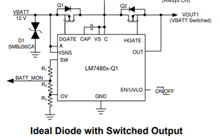
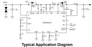
Other Parts Discussed in Thread: LM7480-Q1, LM74910-Q1

Hi TI expert,

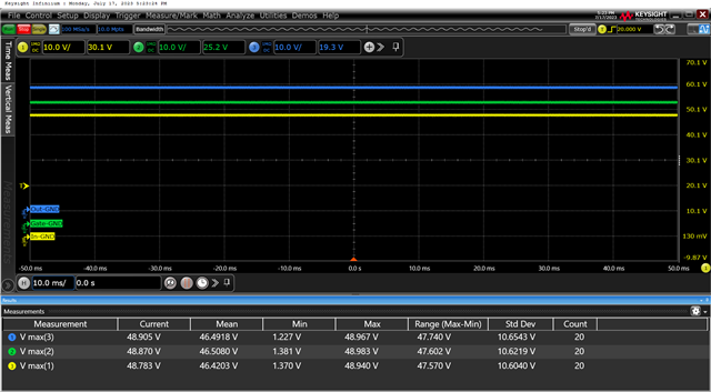
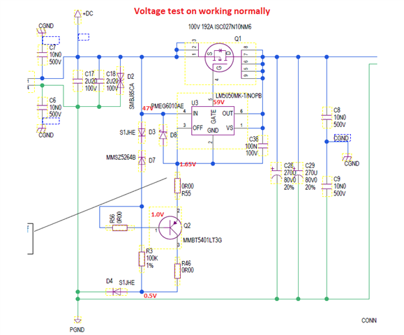
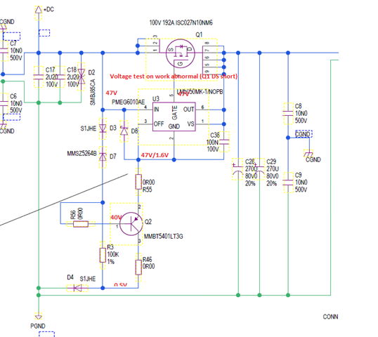
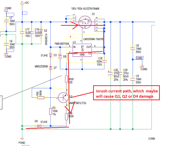
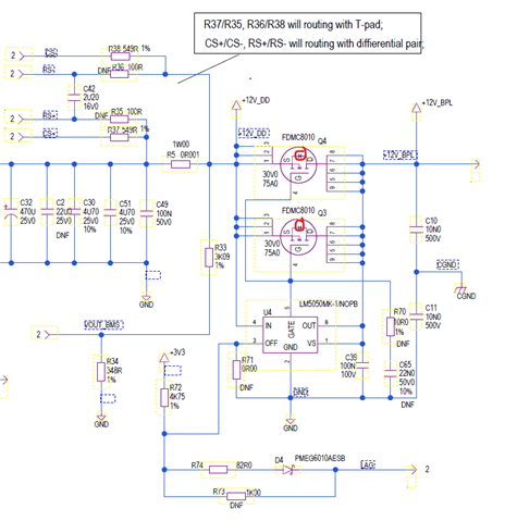
We are using LM5050-1 on our PSU's input reverse polarity protection and find some damage after surge test.

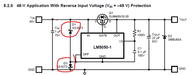
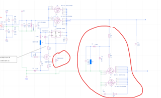
Their schematic is as below.

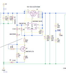
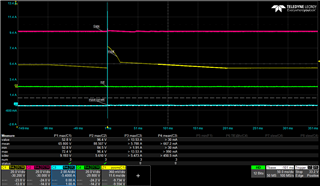
The surge voltage is negative, ~ 1000V from input side as below figure.

we found Q1's DS are short, D7/D8 are also damaged, which will make input (IN vs GND) are short and very big big dangerous current, could you please help to review if the schematic has some problem and give some advice to solve this surge test damage.

Thank you!

Best regards,

Bruce

  • Hi Bruce,

    Is D4 also damaged ?

    If yes, this means that D4 is not able to withstand the reverse voltage then subjecting LM5050-1 to negative voltage which it cannot withstand. 

    Can you share waveform captures with IN-GND, OUT-GND, GATE to GND (all signals captured w.r.t IC GND)

  • Hi Praveen,

    I am sorry for delay reply, the attached is my test waveform for you checking:

    actually, we total have 4pcs samples fail, detail fail symptom as below:

              sample 1: as my description below, Q1's DS is short, D7/D8/D4 is damage;

              sample 2&3&4: only Q1 DS is short, others component is ok.

    Q1 is infineon ISC027N10NM6, which have 100V/192A, generally speaking, it is a stronger FET;

    one more question for LM5050 application in my schematic, only reverse input voltage (VIN = –48 V) protection, no inrush current protection, right? if we add RC on gate pin to turn on FET slowly, which can reduce inrush current?

    on our actually application, we need always hot pull/plug PSU input cable, is it possible inrush current to make this failure.

    Hope get your good comments, thanks!

    Best regards,

    Bruce Lin

  • Hi Bruce,

    For inrush current control, you will need a FET in load switch orientation. The FET in Ideal Diode orientation cannot block/ limit the forward current due to its body diode.

    For Input Reverse polarity Protection +  Reverse Current Blocking + Inrush Current control, you will need a device like LM7480-Q1 which can drive two back-to-back FETs as shown below. 

    The root cause of damage of LM5050-1 is probably the 'voltage ringing> FET VDS rating or other components rating' during hot plug.

  • Hi Praveen,

    thanks for your comments, I have a quick skip for LM7480-Q1, which input voltage is 3V ~ 65V, However, our PSU's input voltage range is 36V ~ 72V,

    do you have other option for me, thanks!

    Best regards,

    Bruce

  • Hi Bruce,

    If reverse current blocking is not required and just Reverse polarity Protection + Inrush Current control are sufficient, then you can consider using TPS4811x-Q1family of devices in the below configuration.

  • Hi Praveen,

    our PSU will be used on telecom system, so reverse current blocking is not required, but we need reverse polarity protection and inrush current control;

    I want to  have better understanding for TPS4811x-Q1familly:

      1. Q1 will be used inrush current control, Q2 will be used reverse polarity protection, right?

      2. how to set INP/INP_G, can we use divider resistor connect to input voltage directly?

      3. can we not use DIODE for temp monitor?

      4. is necessary for Pre-charge supply input?

      5. TPS4811x-Q1 is a new part, right? is there any special note need I , it's very appreciate if you can share some detail design guide for my design case.

    many thanks!

    Best regards,

    Bruce

  • Hi Praveen,

    for previous discussion for LM5050 design, I still want to have more better understanding to find root cause:

    below is some voltage value on normal and abnormal work condition:

    1. voltage test result on work normal condition (Q1 is ok);

    2. voltage test result on work abnormal condition (Q1 DS short)

    3. why sometime Q1 DS is short, sometime Q2/D4 is damage, maybe there is some inrush current as below picture showing;

    4. base on above analysis, can we fix this issue if optimize my original design as below picture showing

    Best regards,

    Bruce

  • Hi Bruce,

    The abnormal condition is a negative surge voltage of ~ 1000V from input side, right?

    you will have to capture waveform with IN-GND, OUT-GND, GATE to GND signals when the transient is applied and not during steady state condition.

  • Hi Praveen

    I continue to do some testing today, now, I think this issue is sure caused by inrush current while hot insert DC cable,

    below is my detail test waveform, you can find thin input current is very big, which is more than 10x normal input current, unfortunately, my PSU are damage (U20 pin 3 and pin 5 are short) and I forgot save normal work waveform.

    Anymore, if I still want to use LM5050 for reverse input voltage protection, and add NMOS on negative line for inrush current protect, detail as below, do you thick below design is ok? my confuse point is the inrush circuit should be before reverse input voltage protection circuit or after it, which one is better?

    BTW, I want to  have better understanding for TPS4811x-Q1familly:

      1. Q1 will be used inrush current control, Q2 will be used reverse polarity protection, right?

      2. how to set INP/INP_G, can we use divider resistor connect to input voltage directly?

      3. can we not use DIODE for temp monitor?

      4. is necessary for Pre-charge supply input?

      5. TPS4811x-Q1 is a new part, right? is there any special note need I , it's very appreciate if you can share some detail design guide for my design case


    Best regards,

    Bruce

  • Hi Bruce,

    Let me review your comments and get back to you within couple of days.

  • Hi Praveen,

    is there any good news, many thanks!

    Best regards,

    Bruce

  • Hi Bruce,

    The current spike in the waveform you shared is during input hotplug and this is because the current is drawn from input to charge the output capacitors of the board. As there is no load switch / Hotswap FET to limit the inrush current, the current peak will be there during hotplug.

    It is  better to have LM5050-1 (for reverse current Blocking + Input revrese polarity protection) first in the power path followed by a separate circuit for inrush current limiting.This will help protect the Input revrese polarity protection circuit from seeing input negative voltage during Input revrese polarity conditions.

    Regarding questions on TPS4811x-Q1familly, please raise a separate e2e query as expert on that device will reach out to you. 

  • Hi Praveen,

    do you say LM5050-1 can work both ways, which also have Hotswap inrush current protection, right? if yes, can you show how to design it, thanks!

    Bruce 

  • Hi Bruce,

    Sorry for the confusion. It is  better to have LM5050-1 (for reverse current Blocking + Input revrese polarity protection) first in the power path followed by a separate circuit for inrush current limiting.

    This will help protect the Input revrese polarity protection circuit from seeing input negative voltage during Input revrese polarity conditions.

  • Hi Praveen,

    ok, thank for your great support, it's very clear for me now, thanks!

    Best regards,

    Bruce

  • Hi Praveen,

    one more question also need you help, on our PSU, we also use LM5050 for OR-ing and output hot swap control, detail as below picture showing.

    my confuse is the "LAG" will short to GND on backplane, if not insert PSU to backplane, which mean off pin will pull up to 3.3V, and then gate pin will output low voltage level to turn off Q3/Q4, however, there is some body diode for Q3/Q4, so there are still some current go to  the drain pins of mosfet, right? if yes, that's mean no hot-swap function anymore.

    do you have any good comment for this, thanks!

  • Hi Bruce, 

    Yes, your understanding is correct. There is no control  on forward current when you are using just ORing/ Ideal diode FETs which have their source connected to input and drain connected to output. 

    For inrush current control/ Hotswap control you will need a FET is reverse orientation that is its Drain connected to input and Source connected to output. 

    So, over all you will need devices like LM7480-Q1 or LM74910-Q1 which can drive back-to-back FETs as shown below.


  • Hi Praveen,

    thanks for your good comments,  our PSU is 12.2V/450W output, and the OVP point is about 15.6V, how should setting R1/R2/R3 value?

    Best Regards,

    Bruce Lin

  • Hi Bruce lin,

    Please refer to the datasheet '10 Applications and Implementation' for understanding on how to calculate the component values.