Thank you for your time today.
We're looking to use TPS61196 in an application, and I'm having an issue getting the regulator to startup. To note, on both chips VDD hits ~6V when (simultaneously) enabled and PWM1-6 appear to function, albeit with VOUT at VIN instead of boosting.
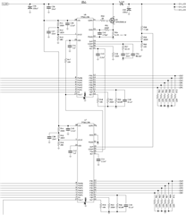
While still investigating, I'd appreciate a sanity check on my values to ensure I'm not out in left field looking at the sky. Below are the relevant portions of the schematic and a page whipped up for calculation.
Some quick questions (re: datasheet, relevant excerpts in link):
- I believe I'm misinterpreting the equation in figure 1, as it looks to contradict Table 1/Figure 4. For 400kHz switching, I definitely should be using 100k Ohms, not 100 Ohms?
- For the "Multi-Chip Operation In Parallel" diagram in figure 22, some components from the single chip layout are omitted (C8, R13-18). Is this intentional or is the drawing meant to only illustrate the connections with the heavier weighted red lines?
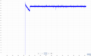
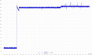
- Assuming the presence of R13-18, if C8 was omitted, could the (admittedly possibly unstable?) startup exhibit the behavior shown in the graph below? Apologies for lack of ISNS data, will check today.
- Generally, does anything else in the schematic or linked page stand out as incorrect?
Thank you again,
Elliot Kampa
Calculations: https://dev.ilot.net/TahPei3ahP/tps61196_demo1/tps61196.html
Schematic excerpt:
Startup issue capture, Vout @ L1: