This thread has been locked.
If you have a related question, please click the "Ask a related question" button in the top right corner. The newly created question will be automatically linked to this question.
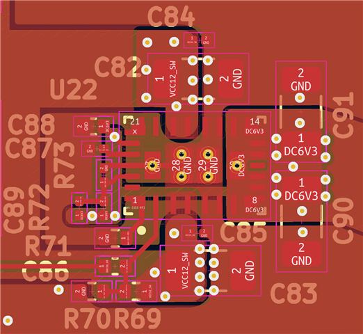
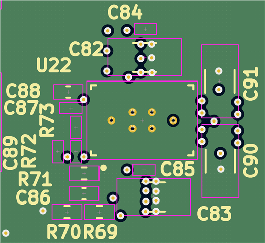
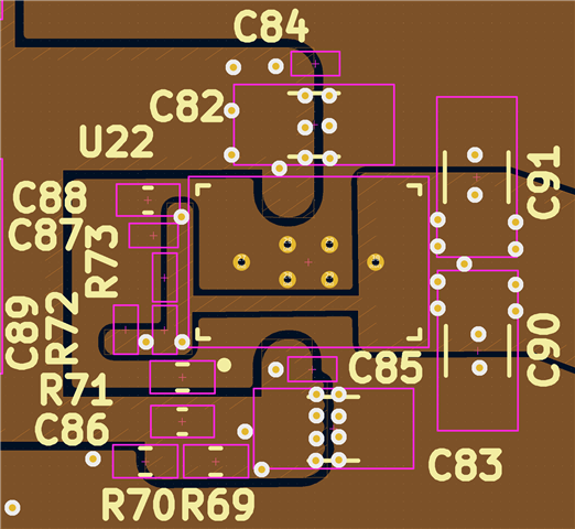
For the chip TPSM63602,
1. the data sheet give a recommended layout, but that does not connect the VOUT pins to the FB and VLDOIN pins,
I want to know what is the recommended approach to connect them? using via on another layer? or trace from outside;
2 for the VIN on the two side, should I connected myself on the pcb board or they are internal connected?
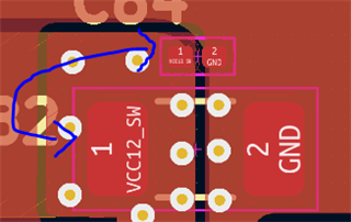
3. To connect the VCC to PGND, the data sheet asking for a high quality 1-μF ceramic capacitor, will a X5R considered as a high quality capacitor? Such as GRM033R61C105ME15D good enough?
Hi Gang,
1. FB is connected to VOUT through a via on another layer.
You're right that VLDOIN is not connected to anything. It should be connected to GND or VOUT depending on what output voltage is needed for the application. You can connect it to VOUT with a via.
2. It looks like they are connected on another layer. There's 3 vias on each VIN plain.
3. Going off of a more modern datasheet, they define high quality as X7R or better. I would personally recommend using an X7R or better. However, the TPSM63603EVM does use an X5R (EMK105BJ105KVHF) for that design which was tested and validated by our team.
Thanks,
Andrew
Hi Gang,
Yeah, GRM033R61C105ME15D should be fine. I trust that a Japanese MLCC manufacturer like Murata or TDK to provide a reliable part.
For the layout it looks good. My only suggestion would be to swap the position of C84 and C82. That way the Low ESR component is as close to VIN as possible.
Thanks,
Andrew