This thread has been locked.

If you have a related question, please click the "Ask a related question" button in the top right corner. The newly created question will be automatically linked to this question.

LM25143-Q1: VCC behaver related to VCCX pin setting, and how to current limit setting

Part Number: LM25143-Q1

The followings are question for LM25143-Q1 from a customer.

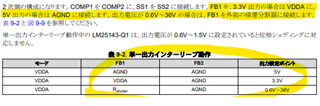
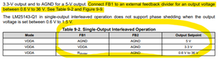
1. データーシートの図9.9のようなインターリーブで 3.3V出力の仕様をWebenchで回路生成させるとVCCXはGND接続となります。
一方、図9.9(DS_P33)でのVCCXはVout(3.3V)に接続されています。この違いは何が原因ですか?
If you generate a simulation bench circuit with Webench for 3.3V output specifications with interleaving as shown in Figure 9.9 of the datasheet, VCCX is connected to GND.
On the other hand, VCCX in Figure 9.9 (Datasheet, Page.33) is connected to Vout (3.3V). What causes this difference?

2. ”VCCX > 4.3V の場合、VCCX は VCC に内部で接続され、内部の VCC レギュレータはディセーブルになります。”とデーターシート(P6)記載あります。前記の質問1.ではVCCXが3.3Vに接続、又はGNDに接続先されたケースですが、いずれもVCCXは4.3V未満です。接続先は異なりますが、どちらのケースもVCCは同じ状態でしょうか?
"When VCCX > 4.3V, VCCX is internally connected to VCC and the internal VCC regulator is disabled." is stated in the datasheet (P6). In the above question 1, VCCX is connected to 3.3V or connected to GND, but in both cases VCCX is less than 4.3V. The connection destination is different, but is VCC in the same state in both cases?

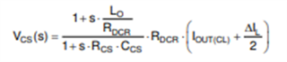
3. インダクタ DCR 電流センシング方式で過電流値の設定は式12(DS_P29)と思われます。
式12が理解できません。 具体的に例えばインターリーブ3.3V 20AでLo=470nH DCr=3.6mΩのケースでご説明頂けると助かります。
式の記述に関する質問もあります。Vcs(s)は電圧ではないのですか?単位はs(秒)となっています。それとも検出時間ですか? また式の中にある”s”も何を指しているのか不明です。(1+s*Lo/Rdcrのところにあるs)
The setting of the overcurrent value in the inductor DCR current sensing method seems to be Equation 12 (DS_P29).
I don't understand equation 12. It would be helpful if you could give a specific example of a case where Lo = 470nH DCr = 3.6mΩ at interleaved 3.3V 20A.
I also have a question about writing expressions.  Isn't Vcs(s) a voltage? The unit is s (seconds). Or is it detection time?  Also, it is unclear what the "s" in the formula refers to. (1+s*Lo/s at Rdcr)

Best Regards, Taki

  • 以下、回答します。
    PLS see my answer in below.

    1. まずVCCXに関わる動作の確認から述べます。VCCXに4.3Vを超えた電圧を外部から印可しますと、内部使用されるVCC電圧を内部Regualatorから給電される状態からVCCX Pinからの給電に切り替わります。
    Webenchの例では、VCCXをGNDに接続する事により、明示的にVCCへの電力供給に内部Regulatorを使用する事を示しています。
    一方、図9.9の例では、可能であれば外部電源であるVout2をVCCへの供給のために基本的に使用する事を意図しています。
    下記に示すデータシート図9.2にあるように、FB1 PinとFB2 Pinの設定により、Vout2の出力電圧は変わります。
    図9.9の結線を使うと、Vout2の出力電圧設定次第で、電圧が十分高い設定だとVCCへVOUT2から電圧供給され、VCC2の設定がが低いとVCCへの給電はVOUT2でなく、内部Regulatorから行われます。
    この点がWebenchで自動生成される回路と、図9.9の回路、両者の違いです。

    First, let's check the operation related to VCCX. When a voltage exceeding 4.3V is applied to VCCX from the outside, the VCC voltage used internally switches from being fed from the internal regulator to feeding from the VCCX pin.
    The Webench example explicitly shows using the internal regulator to power VCC by connecting VCCX to GND.
    On the other hand, the example in Figure 9.9 is primarily intended to use the external power supply, Vout2, to supply VCC if possible.
    As shown in the datasheet Figure 9.2 below, the setting of the FB1 Pin and FB2 Pin changes the output voltage of Vout2.
    Using the wiring in Figure 9.9, depending on the Vout2 output voltage setting, if the voltage is set high enough, VCC will be supplied from VOUT2, and if VCC2 is set low, VCC will be supplied from the internal regulator instead of VOUT2. It is done.
    This is the difference between the circuit automatically generated by Webench and the circuit in Figure 9.9.

    2. ご認識の通りです。

    Your understanding is correct.

    3. 式12のVcs(s)は、インダクタ電流に対するセンスコンデンサCcsの両端電圧Vcsを表す伝達関数です。
    Vcs(s)の単位は電圧[V]です。ここでsは複素周波数[1 / 秒]で、Vcs(s)はsを引数とする複素関数です。sは伝達関数における一般的な表記ですが、この点は表記的にややこしい部分でもあります。

    以下、過電流値の設定について説明します。
    過電流設定ポイントのインダクタ電流に対してVcsの検出電圧閾値73mVとなるRDCRをもつインダクタを選定、又は設計します。Vout=3.3V、Lo=470nHであれば(更にfsw=2.2MHz、Vinを12Vと仮定)、インダクタのピーク電流は(IOUT(CL)+ΔIL/2)= 21.16Aとなり、RDCRは3.6mΩ程度と算出できます。ここで、IOUT(CL) = 20A、ΔIL = (Vin – Vout)・Ton / Lo、Ton = 1 / fsw・(Vout / Vin)です。
    下記、式12において、

    (1+s(Lo/ RDCR))/(1+s(Rcs・Ccs))を1としてVcs(s) = RDCR・(IOUT(CL) + ΔIL/2)に上記値を代入すると、RDCRの値を得る事ができます。
    また、(1+s(Lo/ RDCR))/(1+s(Rcs・Ccs))を1とする際に考慮すべきは、下記に示すデータシートP.28の記述です。

    この記述にある(Lo / RDCR)と(Rcs・Ccs)はそれぞれ、LoとRDCRの枝路(インダクタ側)と、RcsとCcsからなる枝路(センスコンデンサ側)に対する時定数です。
    インダクタ側の時定数に対して、センスコンデンサ側の時定数を十分小さくすればインダクタのスイッチングリプル電流にVcsが追従し、ピーク電流で過電流が検出できます(上側の行の記述)。それと逆にインダクタ側の時定数に対して、センスコンデンサ側の時定数を十分大きくすれば、スイッチングリプル電流に追従せずに、出力電流(DCレベル、IOUT(CL) + ΔIL/2でなくIOUT(CL) )で検出できます(下側の行の記述)。通常であればピークで検出するケースが多いかと思います。よって、式12はIOUT(CL)でなく、(IOUT(CL) + ΔIL/2)を含んだ表現になっています。

    以下は補足説明です。
    上記式の記述がある同じ項目に、“s ドメインのセンス・コンデンサ間の電圧降下を計算するには、式 12 を使用します。”との文言がありますが、この文言がtドメイン(時間ドメイン、時間領域)の関数、つまり時間tを入力とした電圧値の時間的な関数ではなく、sドメイン(s領域、複素周波数領域)で語られる伝達関数であるという事を意味しています。ちなみに複素周波数は、複素数の絶対値で周波数を、偏角で位相(シフト)を表します。

    ここで単位に関して記述しておきます。下記がその式12ですが、

    単位に関して申しますと右辺の分母、分子に現れる(Rcs・Ccs)や(Lo / RDCR)は時定数を表し、単位として秒の次元を持ちます。よって、右辺の分数部分(1+s(Lo/ RDCR))/(1+s(Rcs・Ccs))は無名数となり、右辺残りのRDCR・(IOUT(CL) + ΔIL/2)が電圧の次元を持ちます。よって、左辺のVcs(s)も電圧の次元を持ちます。

    インダクタ電流に対するVcsの伝達関数であれば、一般的にはインダクタ電流ILを入力とした時のセンス電圧Vcsの応答を表しますが、式12ではILの代わりに(IOUT(CL)+ΔIL/2)となっており、過電流設定ポイントにおける式を表現しています。

    電流センシングにおいてDC分(インダクタ電流ILと検出電圧VcsのDCレベル、又は上記2つの時定数に対して十分低い周波数)について考える時は、右辺においてs=0を代入します。VcsはRDCR・(IOUT(CL) + ΔIL/2)で決まるので、過電流設定ポイントIOUT(CL)時のインダクタピーク電流にVcsの検出電圧閾値73mVとなるRDCRをもつインダクタを選定、又は設計します。

    Vcs(s) in Equation 12 is the transfer function representing the voltage Vcs across the sense capacitor Ccs with respect to the inductor current.
    The unit of Vcs(s) is voltage [V]. where s is the complex frequency [1/sec] and Vcs(s) is the complex function with s as its argument. s is a common notation for transfer functions, but this is where the notation gets confusing.

    The following describes how to set the overcurrent value.
    Select or design an inductor with an RDCR that provides a Vcs detection voltage threshold of 73mV for the inductor current at the overcurrent set point. If Vout = 3.3V, Lo = 470nH (assuming fsw = 2.2MHz and Vin = 12V), the inductor peak current will be (IOUT(CL) + ΔIL/2) = 21.16A and the RDCR will be 3.6mΩ. increase.
    where, IOUT(CL) = 20A, ΔIL = (Vin – Vout)·Ton/Lo, Ton = 1/fsw·(Vout/Vin).

    In Equation 12 below,

    If (1+s(Lo/ RDCR))/(1+s(Rcs・Ccs)) is 1 and the above value is substituted for Vcs(s) = RDCR・(IOUT(CL) + ΔIL/2), RDCR can get the value.

    Also, when setting (1+s(Lo/ RDCR))/(1+s(Rcs・Ccs)) to 1, the description on page 28 of the data sheet shown below should be considered.

    (Lo/RDCR) and (Rcs · Ccs) in this description are the time constants for the branch consists of Lo and RDCR (inductor side) and the branch consists of Rcs and Ccs (sense capacitor side), respectively.
    If the time constant on the sense capacitor side is made sufficiently smaller than the time constant on the inductor side, Vcs will follow the switching ripple current of the inductor, and overcurrent can be detected from the peak current (description in the upper line). Conversely, if the time constant on the sense capacitor side is sufficiently large relative to the time constant on the inductor side, the output current (DC level, IOUT(CL) + ΔIL/2 instead of IOUT (CL) ) (description in the lower line). I think there are many cases that the peak current is used for detection. Therefore, Equation 12 includes (IOUT(CL) + ΔIL/2) instead of IOUT(CL).

    Below is a supplementary explanation.
    In the same entry where the above equation is written, there is a sentence "To calculate the voltage drop across the sense capacitor in the s domain, use Equation 12." , time domain), that is, it is not a function of the voltage value with time t as an input, but a transfer function that is told in the s domain (s domain, complex frequency domain). For complex frequency, the absolute value of the complex number represents the frequency, and the angle of argument represents the phase (shift).

    Next, Let me explain about the units.  The formula 12 is shown in below again.

    Regarding units, (Rcs・Ccs) and (Lo / RDCR) appearing in the denominator and numerator on the right side represent the time constant, and have the dimension of seconds as the unit. Therefore, the fractional part on the right side (1+s(Lo/ RDCR))/(1+s(Rcs・Ccs)) is an unitless number, and the remaining RDCR・(IOUT(CL) + ΔIL/2) on the right side has the dimension of voltage. Therefore, Vcs(s) on the left side also has the voltage dimension.

    If it is the transfer function of Vcs with respect to the inductor current, it generally expresses the response of the sense voltage Vcs when the inductor current IL is inputted. And it also represents the equation at the overcurrent set point.

    When considering the DC component in current sensing - the DC level of the inductor current, IL and the detection voltage, Vcs, or a sufficiently low frequency relative to the above two time constants, substitute s=0 on the right side.  Since Vcs is RDCR ( IOUT(CL) + ΔIL/2), select or design an inductor that has an RDCR that gives the Vcs detection voltage threshold of 73mV for the inductor peak current at the overcurrent set point IOUT(CL).

    Best Regards, Taki

  • Hello Taki,

    Let me get an engineer to look into this and get back to you soon.

    Regards,

    Jimmy

  • Hi Jimmy,
    Thank you for your reply.

    I described my answer for the customer's questions, but if you have any additional comment, it helps me and my customer.

    Best Regards, Taki 

  • Hello Taki

    Sorry for the late response. I was out of office. 

    1. Your answer is correct. The  Fig 9-9 example is confusing now because FB1/FB2 connection matches with 3.3V configuration while VCCX connection matches with 5.0V configuration

    2. Your answer is correct

    3. In the equation 12, S represent Laplace domain (S=2*pi*j)

    -EL