This thread has been locked.

If you have a related question, please click the "Ask a related question" button in the top right corner. The newly created question will be automatically linked to this question.

TPS65987D: can TPS65987D and HD3SS3220 co-exist?

Part Number: TPS65987D
Other Parts Discussed in Thread: HD3SS3220

HI,dear.

I want to use TPS65987D (for DR_SWAP) combined with HD3SS3220 (for MUX), which both of their CC lines connect together to the same pin of Type-c receptacle.

Because HD3SS3220 device does not support PD communications over CC lines and integrate Rp/Rd so then influence the voltage of CC , does it cause conflict when TPS65987D communicate to tablet?

Thanks

  • Hi,

    Connecting both the TPS65987D and HD3SS3220 to the CC lines in your system will not be an issue for the TPS65987D but can be an issue for the far end device. Both controllers will receive CC communication from the far end device through the USB C port, but USB PD messages are not supported by the Type C controller HD3SS. The Type C controller could respond with a not supported message to the far end device because an unknown PD message meant for the PD controller was received. This will cause problems with the far end device.

    We recommend using our PD controller (DR_Swap) in conjunction with a TUSB device, such as TUSB546, for redriver support (SS Mux included). This design is what is seen on our EVM.

    Best Regards,

    Alex

  • Hi, dear. Thank for your recommendation.

    Sorry for the another question about flash.

    a).There is no flash chip but have an EC controller connected to TPS65987D by I2C on my board.

    Since there is EC that can program TPS65987D, is it still necessary to set Boot mode by ADCIN1 and SPI_MISO?

    b). There is flash chip directly connected to TPS65987D and have an EC controller connected to TPS65987D by I2C on my board.

    Because there is no flash programmer, the flash is empty. Can I program Boot Code and Patch Bundle to the flash by the I2C between EC controller and  TPS65987D?

    Thank you again!

  • Hi,

    a.) If the TPS65987D will ever need to boot up in dead battery mode (unpowered sink), you should configure the SPI_MISO and ADCIN1 pins as needed. This will allow you to enable certain power switches/power paths before VIN_3V3 is present or a configuration is loaded to the PD. You do not have to use these configurations if you do not need the functionality they enable or do not need to start in dead battery mode.

    b.) If your Flash chip uses I2C, you can use the same I2C lines connected to TPS65987D to connect to the Flash. Just ensure EC does not interfere during Flash programming (leave EC unpowered if possible when programming flash, just power the Flash separately). If your Flash is a SPI flash, you will need to use SPI.

    Best,
    Alex

  • HI, dear.

    As to b.), my flash chip uses SPI connected to TPS65987D. You said "Just ensure EC does not interfere during Flash programming (leave EC unpowered if possible when programming flash, just power the Flash separately)". Because there is no flash programmer and let me leave EC unpowered, how to program the flash chip? 

    Considering mass production later, it is inconvenience that program the flash one by one.

    So i want to take TPS65987D as a bridge, (ie. EC send Boot Code and Patch Bundle to TPS65987D by I2C,  then TPS65987D send them to flash chip by SPI to achieve the purpose of programming the flash). Is it possible?

    Thank you

  • Hi,

    My apologies for the confusion. Yes, for production I would not recommend powering the Flash separately. 

    Patch Bundle Update Tasks (PTCx), which are 4CC commands sent from the EC to the PD controller while in patch mode, is meant to program the SRAM directly on the PD controller. To program the flash using SPI with the PD controller as a bridge, you can use the Flash Erase/Load/Write/Read I2C 4CC commands detailed in the technical reference manual (FLrr, FLer, FLrd, FLad, FLwd, FLem, FLvy). These commands will allow you to send the patch through the PD controller and then through SPI to the flash.

    Please see this application note for guidance:

    slvae21a.pdf

    Best,

    Alex

  • Hi, dear.

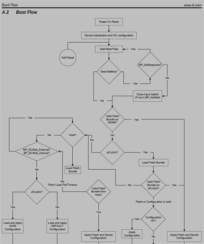
    Although I see the boot FLOW,  I have a puzzle. Two preconditions as below:

    1.If there is a SPI FLASH and it has been programmed.

    2. ADCIN1 is set to the value between 0.30 and 0.38, the chip will enter the state of Infinite Wait which device infinitely waits in boot state for configuration information. 

    When powering up(VIN_3V3 is present), there are two kinds of possible boot flow,  please tell me which is right?

    aaa. Boot from external flash as picture shown below, no use ADCIN1

    bbb. according to the setting of ADCIN1, the chip prior to enter the the state of Infinite Wait and then load the Boot Code and Patch Bundle stored in the FLASH.

     Why I think in this way is that if aaa flow is right, there is no necessary to have the state of "Infinite Wait". You can use either the external flash or Valid Patch Bundle on SRAM

  • Hi,

    If VIN_3V3 is present, the PD controller will not boot up in dead battery mode. Hence, scenario aaa will occur. The dead battery configuration, infinite wait, will be ignored. You are correct that infinite wait is not necessary when not in dead battery mode.

    Best,

    Alex