Hi team,
Would you please help comment on the difference design margin between these two circuits?
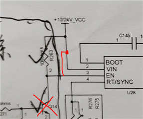
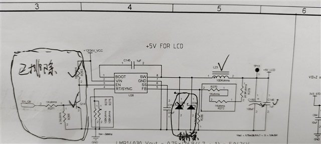
Below 1st figure had some abnormal working conditions compared with 2nd figure. Both of the parameters are the same except for adding the voltage detecting block on the left side.

Vin =12V, Vout=5V, if under 1st schematic, the output is abnormal. Yellow is output =2V, and sw is purple.

In second schematic, Vin=12V, Vout=5V, SW is normal. and replace the good board LMR14030 to the abnormal board, the IC could not work either. So I think it is related to the design margin of these two circuit. Would you please help comments on it? 300 pcs LMR1430 will occurred 2pcs had this kind of issue.