


In order to comply to a standard, I need to keep certain parts of the circuit separate from others. For the TPS2640, I need to keep all the signal pins at least 0.20mm away from the central ground pad as shown here with the red and green distances.
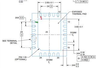
The nominal distance for this seems fine at 0.275mm (Calculated by (4.0 -0.4 - 2.65 - 0.4)/2) for the green gap
However, by assuming the worst case tolerances (casework is only 3.9mm wide, the thermal pad is 2.75mm, and the pin length is 0.5mm), then the gap is only 0.075mm.
This gap seems unrealistically small to me. Would this gap in practice ever be below 0.2mm, or could the tolerances ever stack in this way?
I would use the SOIC-16 variant of this chip where all of these problems go away, but there seems to be a great shortage of the SOIC-16 version for a very long time.
Thanks.
