This thread has been locked.

If you have a related question, please click the "Ask a related question" button in the top right corner. The newly created question will be automatically linked to this question.

TPS6594-Q1: TPS6594 output abnormally in temperature cycle tests

Part Number: TPS6594-Q1
Other Parts Discussed in Thread: TDA4VM-Q1

Hello TI experts,

We are doing temperature cycle tests with our custom boards and find TPS6594 output abnormally. Some information is for you as below.

->The temperature range is from -40°~+85°。 We have reproduced this failure several times. Most of them are in low temperatue.

->Our SOC is TDA4VM-Q1 and we use PDN_0C power solution. That means we use TPS65941213 and TPS65941211.

->When this failure occurs, the test results of PMIC output are as below.

      Voltage/V
  VSYS_3V3   3.3077
PMIC_A VDD_CPU_0V8 BUCK123 0.0000
VDD_MCU_0V85 BUCK4 0.0000
VDD_PHYIO_1V8 BUCK5 0.0031
VDD1_LPDDR4_1V8 LDO1 0.0031
VDD_MCUIO_1V8 LDO2 0.0001
VDA_DLL_0V8 LDO3 0.0001
VDA_MCU_1V8 LDO4 0.046
VRTC_LEOA_1V8 Internal LDOs 1.8030
VINT_LEOA_1V8 Internal LDOs 1.8003
PMIC_B_ENABLE   1.7520
PMIC_B CORE_0V8 BUCK1234 0.0000
RAM_0V85 BUCK5 0.0000
USB_3V3 LDO2 0.0001
VDDIO_1V8 LDO3 0.000

->when this failure occurs, I try to get the access to I2C with an external I2C tool but failed. Maybe PMIC's I2C can not work at that time. However, I dump the registers before this failure occurs and atteched.

Slave Address	Register Address	Register Name	Register Value
0x48	1h	DEV_REV	82
0x48	2h	NVM_CODE_1	13
0x48	3h	NVM_CODE_2	4
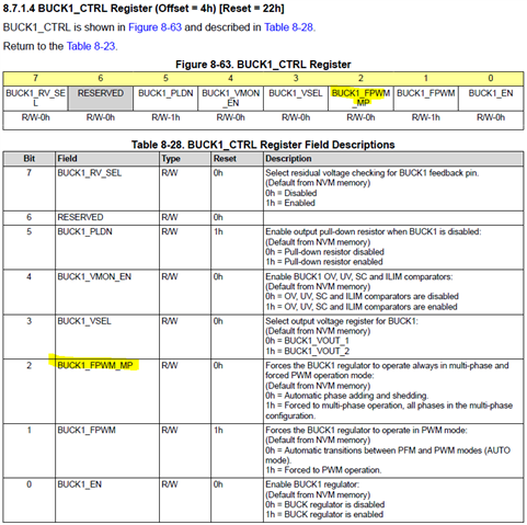
0x48	4h	BUCK1_CTRL	31
0x48	5h	BUCK1_CONF	2B
0x48	6h	BUCK2_CTRL	20
0x48	7h	BUCK2_CONF	2B
0x48	8h	BUCK3_CTRL	30
0x48	9h	BUCK3_CONF	2D
0x48	Ah	BUCK4_CTRL	31
0x48	Bh	BUCK4_CONF	2B
0x48	Ch	BUCK5_CTRL	31
0x48	Dh	BUCK5_CONF	1B
0x48	Eh	BUCK1_VOUT_1	41
0x48	Fh	BUCK1_VOUT_2	37
0x48	10h	BUCK2_VOUT_1	37
0x48	11h	BUCK2_VOUT_2	37
0x48	12h	BUCK3_VOUT_1	FD
0x48	13h	BUCK3_VOUT_2	FD
0x48	14h	BUCK4_VOUT_1	41
0x48	15h	BUCK4_VOUT_2	41
0x48	16h	BUCK5_VOUT_1	B2
0x48	17h	BUCK5_VOUT_2	B2
0x48	18h	BUCK1_PG_WINDOW	1B
0x48	19h	BUCK2_PG_WINDOW	1B
0x48	1Ah	BUCK3_PG_WINDOW	3F
0x48	1Bh	BUCK4_PG_WINDOW	1B
0x48	1Ch	BUCK5_PG_WINDOW	1B
0x48	1Dh	LDO1_CTRL	31
0x48	1Eh	LDO2_CTRL	31
0x48	1Fh	LDO3_CTRL	31
0x48	20h	LDO4_CTRL	31
0x48	/		0
0x48	22h	LDORTC_CTRL	0
0x48	23h	LDO1_VOUT	38
0x48	24h	LDO2_VOUT	38
0x48	25h	LDO3_VOUT	10
0x48	26h	LDO4_VOUT	38
0x48	27h	LDO1_PG_WINDOW	1B
0x48	28h	LDO2_PG_WINDOW	1B
0x48	29h	LDO3_PG_WINDOW	1B
0x48	2Ah	LDO4_PG_WINDOW	1B
0x48	2Bh	VCCA_VMON_CTRL	21
0x48	2Ch	VCCA_PG_WINDOW	3F
0x48	31h	GPIO1_CONF	20
0x48	32h	GPIO2_CONF	40
0x48	33h	GPIO3_CONF	58
0x48	34h	GPIO4_CONF	C8
0x48	35h	GPIO5_CONF	29
0x48	36h	GPIO6_CONF	28
0x48	37h	GPIO7_CONF	38
0x48	38h	GPIO8_CONF	78
0x48	39h	GPIO9_CONF	1
0x48	3Ah	GPIO10_CONF	D8
0x48	3Bh	GPIO11_CONF	43
0x48	3Ch	NPWRON_CONF	19
0x48	3Dh	GPIO_OUT_1	0
0x48	3Eh	GPIO_OUT_2	1
0x48	3Fh	GPIO_IN_1	40
0x48	40h	GPIO_IN_2	0F
0x48	41h	RAIL_SEL_1	5A
0x48	42h	RAIL_SEL_2	96
0x48	43h	RAIL_SEL_3	5
0x48	44h	FSM_TRIG_SEL_1	1E
0x48	45h	FSM_TRIG_SEL_2	1
0x48	46h	FSM_TRIG_MASK_1	55
0x48	47h	FSM_TRIG_MASK_2	55
0x48	48h	FSM_TRIG_MASK_3	15
0x48	49h	MASK_BUCK1_2	0
0x48	4Ah	MASK_BUCK3_4	0
0x48	4Bh	MASK_BUCK5	0
0x48	4Ch	MASK_LDO1_2	0
0x48	4Dh	MASK_LDO3_4	0
0x48	4Eh	MASK_VMON	0
0x48	4Fh	MASK_GPIO1_8_FALL	FF
0x48	50h	MASK_GPIO1_8_RISE	FF
0x48	51h	MASK_GPIO9_11	3F
0x48	52h	MASK_STARTUP	11
0x48	53h	MASK_MISC	2
0x48	54h	MASK_MODERATE_ERR	20
0x48	56h	MASK_FSM_ERR	0
0x48	57h	MASK_COMM_ERR	0
0x48	58h	MASK_READBACK_ERR	0
0x48	59h	MASK_ESM	3F
0x48	5Ah	INT_TOP	0
0x48	5Bh	INT_BUCK	0
0x48	5Ch	INT_BUCK1_2	0
0x48	5Dh	INT_BUCK3_4	0
0x48	5Eh	INT_BUCK5	0
0x48	5Fh	INT_LDO_VMON	0
0x48	60h	INT_LDO1_2	0
0x48	61h	INT_LDO3_4	0
0x48	62h	INT_VMON	0
0x48	63h	INT_GPIO	0
0x48	64h	INT_GPIO1_8	0
0x48	65h	INT_STARTUP	0
0x48	66h	INT_MISC	0
0x48	67h	INT_MODERATE_ERR	0
0x48	68h	INT_SEVERE_ERR	0
0x48	69h	INT_FSM_ERR	0
0x48	6Ah	INT_COMM_ERR	0
0x48	6Bh	INT_READBACK_ERR	0
0x48	6Ch	INT_ESM	0
0x48	6Dh	STAT_BUCK1_2	0
0x48	6Eh	STAT_BUCK3_4	0
0x48	6Fh	STAT_BUCK5	0
0x48	70h	STAT_LDO1_2	0
0x48	71h	STAT_LDO3_4	0
0x48	72h	STAT_VMON	0
0x48	73h	STAT_STARTUP	2
0x48	74h	STAT_MISC	0
0x48	75h	STAT_MODERATE_ERR	0
0x48	76h	STAT_SEVERE_ERR	0
0x48	77h	STAT_READBACK_ERR	0
0x48	78h	PGOOD_SEL_1	0
0x48	79h	PGOOD_SEL_2	0
0x48	7Ah	PGOOD_SEL_3	0
0x48	7Bh	PGOOD_SEL_4	0
0x48	7Ch	PLL_CTRL	0
0x48	7Dh	CONFIG_1	0
0x48	7Eh	CONFIG_2	0
0x48	80h	ENABLE_DRV_REG	0
0x48	81h	MISC_CTRL	1B
0x48	82h	ENABLE_DRV_STAT	6
0x48	83h	RECOV_CNT_REG_1	0
0x48	84h	RECOV_CNT_REG_2	0F
0x48	85h	FSM_I2C_TRIGGERS	0
0x48	86h	FSM_NSLEEP_TRIGGERS	3
0x48	87h	BUCK_RESET_REG	0
0x48	88h	SPREAD_SPECTRUM_1	0
0x48	8Ah	FREQ_SEL	0
0x48	8Bh	FSM_STEP_SIZE	0B
0x48	8Ch	LDO_RV_TIMEOUT_REG_1	FF
0x48	8Dh	LDO_RV_TIMEOUT_REG_2	FF
0x48	8Eh	USER_SPARE_REGS	0
0x48	8Fh	ESM_MCU_START_REG	0
0x48	90h	ESM_MCU_DELAY1_REG	0
0x48	91h	ESM_MCU_DELAY2_REG	0
0x48	92h	ESM_MCU_MODE_CFG	0
0x48	93h	ESM_MCU_HMAX_REG	0
0x48	94h	ESM_MCU_HMIN_REG	0
0x48	95h	ESM_MCU_LMAX_REG	0
0x48	96h	ESM_MCU_LMIN_REG	0
0x48	97h	ESM_MCU_ERR_CNT_REG	0
0x48	98h	ESM_SOC_START_REG	0
0x48	99h	ESM_SOC_DELAY1_REG	0
0x48	9Ah	ESM_SOC_DELAY2_REG	0
0x48	9Bh	ESM_SOC_MODE_CFG	0
0x48	9Ch	ESM_SOC_HMAX_REG	0
0x48	9Dh	ESM_SOC_HMIN_REG	0
0x48	9Eh	ESM_SOC_LMAX_REG	0
0x48	9Fh	ESM_SOC_LMIN_REG	0
0x48	A0h	ESM_SOC_ERR_CNT_REG	0
0x48	A1h	REGISTER_LOCK	0
0x48	A6h	MANUFACTURING_VER	8
0x48	A7h	CUSTOMER_NVM_ID_REG	0
0x48	ABh	SOFT_REBOOT_REG	0
0x48	B5h	RTC_SECONDS	0
0x48	B6h	RTC_MINUTES	0
0x48	B7h	RTC_HOURS	0
0x48	B8h	RTC_DAYS	1
0x48	B9h	RTC_MONTHS	1
0x48	BAh	RTC_YEARS	0
0x48	BBh	RTC_WEEKS	0
0x48	BCh	ALARM_SECONDS	0
0x48	BDh	ALARM_MINUTES	0
0x48	BEh	ALARM_HOURS	0
0x48	BFh	ALARM_DAYS	0
0x48	C0h	ALARM_MONTHS	0
0x48	C1h	ALARM_YEARS	0
0x48	C2h	RTC_CTRL_1	0
0x48	C3h	RTC_CTRL_2	E0
0x48	C4h	RTC_STATUS	80
0x48	C5h	RTC_INTERRUPTS	0
0x48	C6h	RTC_COMP_LSB	0
0x48	C7h	RTC_COMP_MSB	0
0x48	C8h	RTC_RESET_STATUS	0
0x48	C9h	SCRATCH_PAD_REG_1	0
0x48	CAh	SCRATCH_PAD_REG_2	0
0x48	CBh	SCRATCH_PAD_REG_3	0
0x48	CCh	SCRATCH_PAD_REG_4	0
0x48	CDh	PFSM_DELAY_REG_1	58
0x48	CEh	PFSM_DELAY_REG_2	9D
0x48	CFh	PFSM_DELAY_REG_3	0
0x48	D0h	PFSM_DELAY_REG_4	0

Could you help analyze what errors have occurred in PMIC base on the information above? Thank you in advance.

  • Hi An,


    The device expert is currently out of the office until 8/9. I will look into finding another, and try to look at finding an answer in the meantime. Please expect a delay in response accordingly.


    Thanks,

    Nicholas

  • Hello An,

    What is VIO_IN when the rails turn off? If VIO_IN isn't provided, I2C communication will not work. 

    What is happening before the PMIC powers down? Does the failure happen during boot or is the PMIC actively running and then suddenly shut down?

  • Hello Michael,

    As below,

    --What is VIO_IN when the rails turn off? If VIO_IN isn't provided, I2C communication will not work. 

    After the abnormal has occurred, I tested the VIO_IN and it's normal.

    --What is happening before the PMIC powers down? Does the failure happen during boot or is the PMIC actively running and then suddenly shut down?

    To be honest, We have not yet observed the instantaneous changes that are happening with the anomaly. We just observed the results for several times. However, I can give you more information about tests. We power on ECU and set champer temperature from -40°~+85°. During the test, ECU will not be powered off. So it maybe a suddenly shut down. Meanwhile, I'm not sure if there are abnormal resets. I'll try to reproduce it and do more records.

    Additionally, could you have some directions or speculations? For example, do you think PMIC has entered the safe recovery state?Does I2C work if PMIC is in recovery state. 

  • Hello An,

    Do you know what temperature the system suddenly shuts down?

    Do you lose I2C communication with both PMICs?

    Additionally, could you have some directions or speculations? For example, do you think PMIC has entered the safe recovery state?Does I2C work if PMIC is in recovery state. 

    I2C communication should work in recovery state. I suspect that something has caused the PMIC to execute a digital reset which does cause loss of communication. Digital resets are extremely rarely when PMIC layout guidelines are followed. Of particular importance is the placement and layout of capacitors for the LDO_VINT.

  • Hello Michael,

    We read its currents and board temperature every 3 minutes. And we find the most abnormality occurs in low temperature, which is from -40℃~-20, but there are also some other temperatures, such as 40 and 90℃.

    Some boards failure occurs in our PV test and I cannot debug it much. Then I try to reproduce it and actually this abnormality occurs twice. I cannot communication with PMIC_A for these 2 tests, but I can communicate with PMIC_B for the first test. I'm not sure there are some test deviation. And I'll reproduce it more to get more details and confirmation.

    Then I have a question for your suspection. If there are a digital reset, will PMIC shut down immediately? Could it reset and power on again? How can we to test for it? Monitor the wave on LDO_VIN?

  • Then I have a question for your suspection. If there are a digital reset, will PMIC shut down immediately? Could it reset and power on again? How can we to test for it?

    Yes the PMIC will shutdown all it's rails immediately. It can not recover without a power cycle of the VCCA supply. In the case where PMIC_B still communicates, please read the interrupt registers. Confirm SPMI_ERR_INT is set to 1. 

  • Hello Michael,

    I have reproduced this abnormality again. I try to communicate with PMICs. PMIC_A can not be accessed, while PMIC_B is ok. I dump all the registers of PMIC_B and show it to you as below. Meanwhile, the register values in normal state are also attached.

    Actually, I see SPMI_ERR_INT is set to 1. Then I have some new questions based on this test results.

    Q1: When SPMI_ERR_INT is set to 1, can we be sure there must be a SPMI err and this err causes PMICs shutdown?I just would like to confirm if there is another possibility,for example PMIC's shutdown occurs firstly due to something and SPMI_ERR_INT is set secondly.

    Q2: We see the I2C of PMIC_A can not work and the one of PMIC_B is ok. So can we think there is something wrong with PMIC_A, while PMIC_B is ok?

    Q3: When SPMI_ERR_INT is set to 1, can we be sure there is a digital reset? Or We can only be highly skeptical, and the layout of capacitors for the LDO_VINT is a more likely direction if digital reset occurs?

    Q4:Is it possible that this issue is related to PMIC power dissipation. For example, if the power dissipation of TDA4 is higher, this problem is more likely to occur.

    To be honest, we have finished 2 rounds of the whole temperature cycle test last year. Then we changed some peripheral chips based on some functions requiremests and do a new temperature cycle test. However, there was no such issue before. But we found the issues occured just during this test. 3 of 6 samples has failed. There is no difference from HW design. It is only possible that the material batch and the build time are different. Another difference is that the power consumption of TDA4 has increased by about 3W.

    Register address Register Name normal state abnormal state
    1h DEV_REV 82 82
    2h NVM_CODE_1 11 11
    3h NVM_CODE_2 3 03
    4h BUCK1_CTRL 31 20
    5h BUCK1_CONF 2B 2B
    6h BUCK2_CTRL 20 20
    7h BUCK2_CONF 2B 2B
    8h BUCK3_CTRL 20 20
    9h BUCK3_CONF 22 22
    Ah BUCK4_CTRL 20 20
    Bh BUCK4_CONF 22 22
    Ch BUCK5_CTRL 31 20
    Dh BUCK5_CONF 1B 1B
    Eh BUCK1_VOUT_1 37 37
    Fh BUCK1_VOUT_2 0 00
    10h BUCK2_VOUT_1 37 37
    11h BUCK2_VOUT_2 0 00
    12h BUCK3_VOUT_1 0 00
    13h BUCK3_VOUT_2 0 00
    14h BUCK4_VOUT_1 0 00
    15h BUCK4_VOUT_2 0 00
    16h BUCK5_VOUT_1 41 41
    17h BUCK5_VOUT_2 0 00
    18h BUCK1_PG_WINDOW 1B 1B
    19h BUCK2_PG_WINDOW 1B 1B
    1Ah BUCK3_PG_WINDOW 0 00
    1Bh BUCK4_PG_WINDOW 0 00
    1Ch BUCK5_PG_WINDOW 1B 1B
    1Dh LDO1_CTRL 31 20
    1Eh LDO2_CTRL 31 20
    1Fh LDO3_CTRL 31 20
    20h LDO4_CTRL 31 20
    / 0 00
    22h LDORTC_CTRL 0 00
    23h LDO1_VOUT F4 F4
    24h LDO2_VOUT F4 F4
    25h LDO3_VOUT 38 38
    26h LDO4_VOUT 38 38
    27h LDO1_PG_WINDOW 1B 1B
    28h LDO2_PG_WINDOW 1B 1B
    29h LDO3_PG_WINDOW 1B 1B
    2Ah LDO4_PG_WINDOW 1B 1B
    2Bh VCCA_VMON_CTRL 21 21
    2Ch VCCA_PG_WINDOW 3F 3F
    0 00
    0 00
    0 00
    0 00
    31h GPIO1_CONF 0 00
    32h GPIO2_CONF 1C 1C
    33h GPIO3_CONF 1 01
    34h GPIO4_CONF 3 03
    35h GPIO5_CONF 20 20
    36h GPIO6_CONF 20 20
    37h GPIO7_CONF 10 10
    38h GPIO8_CONF 0 00
    39h GPIO9_CONF 1 01
    3Ah GPIO10_CONF F8 F8
    3Bh GPIO11_CONF 1 01
    3Ch NPWRON_CONF 19 19
    3Dh GPIO_OUT_1 4 00
    3Eh GPIO_OUT_2 4 00
    3Fh GPIO_IN_1 4 00
    40h GPIO_IN_2 0C 08
    41h RAIL_SEL_1 0A 0A
    42h RAIL_SEL_2 A2 A2
    43h RAIL_SEL_3 6 06
    44h FSM_TRIG_SEL_1 1E 1E
    45h FSM_TRIG_SEL_2 1 01
    46h FSM_TRIG_MASK_1 51 51
    47h FSM_TRIG_MASK_2 55 55
    48h FSM_TRIG_MASK_3 15 15
    49h MASK_BUCK1_2 0 00
    4Ah MASK_BUCK3_4 0 00
    4Bh MASK_BUCK5 0 00
    4Ch MASK_LDO1_2 0 00
    4Dh MASK_LDO3_4 0 00
    4Eh MASK_VMON 0 00
    4Fh MASK_GPIO1_8_FALL FD FD
    50h MASK_GPIO1_8_RISE FD FD
    51h MASK_GPIO9_11 3F 3F
    52h MASK_STARTUP 11 11
    53h MASK_MISC 2 02
    54h MASK_MODERATE_ERR A0 A0
    0 00
    56h MASK_FSM_ERR 0 00
    57h MASK_COMM_ERR A0 A0
    58h MASK_READBACK_ERR 9 09
    59h MASK_ESM 3F 3F
    5Ah INT_TOP 0 A0
    5Bh INT_BUCK 0 00
    5Ch INT_BUCK1_2 0 00
    5Dh INT_BUCK3_4 0 00
    5Eh INT_BUCK5 0 00
    5Fh INT_LDO_VMON 0 00
    60h INT_LDO1_2 0 00
    61h INT_LDO3_4 0 00
    62h INT_VMON 0 00
    63h INT_GPIO 0 00
    64h INT_GPIO1_8 0 00
    65h INT_STARTUP 0 00
    66h INT_MISC 0 00
    67h INT_MODERATE_ERR 0 10
    68h INT_SEVERE_ERR 0 00
    69h INT_FSM_ERR 0 02
    6Ah INT_COMM_ERR 0 00
    6Bh INT_READBACK_ERR 0 00
    6Ch INT_ESM 0 00
    6Dh STAT_BUCK1_2 0 00
    6Eh STAT_BUCK3_4 0 00
    6Fh STAT_BUCK5 0 00
    70h STAT_LDO1_2 0 00
    71h STAT_LDO3_4 0 00
    72h STAT_VMON 0 00
    73h STAT_STARTUP 2 02
    74h STAT_MISC 0 00
    75h STAT_MODERATE_ERR 0 00
    76h STAT_SEVERE_ERR 0 00
    77h STAT_READBACK_ERR 0 00
    78h PGOOD_SEL_1 0 00
    79h PGOOD_SEL_2 0 00
    7Ah PGOOD_SEL_3 0 00
    7Bh PGOOD_SEL_4 0 00
    7Ch PLL_CTRL 0 00
    7Dh CONFIG_1 0 00
    7Eh CONFIG_2 0 00
    0 00
    80h ENABLE_DRV_REG 0 00
    81h MISC_CTRL 18 04
    82h ENABLE_DRV_STAT 8 18
    83h RECOV_CNT_REG_1 0 00
    84h RECOV_CNT_REG_2 0F 0F
    85h FSM_I2C_TRIGGERS 0 00
    86h FSM_NSLEEP_TRIGGERS 0 00
    87h BUCK_RESET_REG 0 1F
    88h SPREAD_SPECTRUM_1 0 00
    0 00
    8Ah FREQ_SEL 0 00
    8Bh FSM_STEP_SIZE 0B 0B
    8Ch LDO_RV_TIMEOUT_REG_1 FF FF
    8Dh LDO_RV_TIMEOUT_REG_2 FF FF
    8Eh USER_SPARE_REGS 0 00
    8Fh ESM_MCU_START_REG 0 00
    90h ESM_MCU_DELAY1_REG 0 00
    91h ESM_MCU_DELAY2_REG 0 00
    92h ESM_MCU_MODE_CFG 0 00
    93h ESM_MCU_HMAX_REG 0 00
    94h ESM_MCU_HMIN_REG 0 00
    95h ESM_MCU_LMAX_REG 0 00
    96h ESM_MCU_LMIN_REG 0 00
    97h ESM_MCU_ERR_CNT_REG 0 00
    98h ESM_SOC_START_REG 0 00
    99h ESM_SOC_DELAY1_REG 0 00
    9Ah ESM_SOC_DELAY2_REG 0 00
    9Bh ESM_SOC_MODE_CFG 0 00
    9Ch ESM_SOC_HMAX_REG 0 00
    9Dh ESM_SOC_HMIN_REG 0 00
    9Eh ESM_SOC_LMAX_REG 0 00
    9Fh ESM_SOC_LMIN_REG 0 00
    A0h ESM_SOC_ERR_CNT_REG 0 00
    A1h REGISTER_LOCK 0 00
    0 00
    80 80
    0 00
    0 00
    A6h MANUFACTURING_VER 8 08
    A7h CUSTOMER_NVM_ID_REG 0 00
    0 00
    0 00
    0 00
    ABh SOFT_REBOOT_REG 0 00
    0 00
    0 00
    0 00
    0 00
    0 00
    0 00
    0 00
    0 00
    0 00
    B5h RTC_SECONDS 0 00
    B6h RTC_MINUTES 0 00
    B7h RTC_HOURS 0 00
    B8h RTC_DAYS 1 01
    B9h RTC_MONTHS 1 01
    BAh RTC_YEARS 0 00
    BBh RTC_WEEKS 0 00
    BCh ALARM_SECONDS 0 00
    BDh ALARM_MINUTES 0 00
    BEh ALARM_HOURS 0 00
    BFh ALARM_DAYS 0 00
    C0h ALARM_MONTHS 0 00
    C1h ALARM_YEARS 0 00
    C2h RTC_CTRL_1 0 00
    C3h RTC_CTRL_2 E8 E8
    C4h RTC_STATUS 80 80
    C5h RTC_INTERRUPTS 0 00
    C6h RTC_COMP_LSB 0 00
    C7h RTC_COMP_MSB 0 00
    C8h RTC_RESET_STATUS 0 00
    C9h SCRATCH_PAD_REG_1 0 00
    CAh SCRATCH_PAD_REG_2 0 00
    CBh SCRATCH_PAD_REG_3 0 00
    CCh SCRATCH_PAD_REG_4 0 00
    CDh PFSM_DELAY_REG_1 0 00
    CEh PFSM_DELAY_REG_2 1D 1D
    CFh PFSM_DELAY_REG_3 0 00
    D0h PFSM_DELAY_REG_4 0 00
  • Hello An,

    You raised a few questions and I will try to answer. Overall, I believe the customer is experiencing some increased noise being injected into the PMIC caused by the higher load demands of the TDA4.  You stated the HW design was tested over a year ago with the lighter load demands. Can you confirm that the layout and placement of the LDO_VINT cap follows the guidelines outlined in the data sheet?

    Q1: When SPMI_ERR_INT is set to 1, can we be sure there must be a SPMI err and this err causes PMICs shutdown?I just would like to confirm if there is another possibility,for example PMIC's shutdown occurs firstly due to something and SPMI_ERR_INT is set secondly.

    I believe PMIC_A is experiencing a digital reset due to the before mentioned noise. During a digital reset, all the rails shut down and both I2C and SPMI communication is lost until a power cycle. PMIC-B reports an SPMI Error because it no longer "sees" PMIC-A. This causes PMIC-B to execute an orderly shutdown. 

    Q2: We see the I2C of PMIC_A can not work and the one of PMIC_B is ok. So can we think there is something wrong with PMIC_A, while PMIC_B is ok?

    Refer to my last answer.

    Q3: When SPMI_ERR_INT is set to 1, can we be sure there is a digital reset? Or We can only be highly skeptical, and the layout of capacitors for the LDO_VINT is a more likely direction if digital reset occurs?

    To be certain that a digital reset is happening, disable the clock monitor of PMIC-A after boot by setting CLKMON_EN=0 after boot. If the PMIC does not shut down during your test, then that would confirm that PMIC-A was experiencing a digital reset.

    Q4:Is it possible that this issue is related to PMIC power dissipation. For example, if the power dissipation of TDA4 is higher, this problem is more likely to occur.

    The increased load of TDA4 could be the reason the issue is seen now but not before. The increased loads means heavier load transients and more phase shedding and adding during operation. This increases the noise on the board. To reduce the noise, set BUCK1 on PMIC-A and PMIC-B to be in forced multi-phase mode, BUCK1_FPWM_MP=1 after boot. 

  • Hello Michael,

    Thank you for your reply. We are checking all the points you mentioned.

    Then, could you share you email address? We are communicating with Daviel and John, who are FAE in North American. I'm not sure you have got in touch. I would also like to loop you in the mails. By the way, what's your location? Maybe we can set up an online meeting if necessary. 

  • Hello Michael,

    Your reply is really detailed one by one. Many thanks.

    I check the layout and placement of the LDO_VINT cap. As the limitation of actual layout, the placement of the LDO_VINT cap can not completely meet the requirements of guideline. So we cannot rule out the influence of LDO_Vin cap until now. It maybe a direction.

    Additional, we cannot reproduce this abnormality stably. It may occur once a day or once 2~3 days. It is not very convenient for investigating issue.

     Also, new questions from me.

    Q1: You mentioned there may be a digital reset if the placement of LDO_VIN cap is wrong. And you also mention the increased load of TDA4 and increased noise could be the reason. Is there something related?

    In other words, if the noise of Buck increases, can it directly lead to a digital reset? Or the buck noise increases → LDO noise increases → digital reset?

    We would like to know if it is a combination of two factors. Or just a seperate factor that has no correlation and each can lead to this issue.

    Q2: We did reproduce this abnormality most (more than 80%) at low temperature (-40℃), and once at 20 ℃, once at 60℃. Does it seem reasonable, combined with your suspection? What are the expected changes for PMIC or PMIC noise?

    Q3: To confirm for your answer to the last Q3. I'm not very clear. You mean if we set CLKMON_EN=0, then PMIC_B(?) will not shutdown if a digital reset happen?

    Q4: Setting BUCK1_FPWM_MP=1 may reduce the noise. We only need to set buck1, not care buck3 and others. Can all the buck follow buck1?

    Q5: Is there any potential reason for digital reset? Just would like to learn more if you have more experience and ideas to share.

  • Q1: You mentioned there may be a digital reset if the placement of LDO_VIN cap is wrong. And you also mention the increased load of TDA4 and increased noise could be the reason. Is there something related?

    In other words, if the noise of Buck increases, can it directly lead to a digital reset? Or the buck noise increases → LDO noise increases → digital reset?

    We would like to know if it is a combination of two factors. Or just a seperate factor that has no correlation and each can lead to this issue.

    Increased load on TDA4 means larger load transient events on CORE and CPU rails  --> Larger transient events means more phase shedding and adding --> more noise caused by bucks --> increased noise on LDO_VINT and internal clock --> increased chance of digital reset.

    So it is a combination of the two factors.

    Q2: We did reproduce this abnormality most (more than 80%) at low temperature (-40℃), and once at 20 ℃, once at 60℃. Does it seem reasonable, combined with your suspection? What are the expected changes for PMIC or PMIC noise?

    Yes, this follows my suspicion because at -40C, the capacitors behave differently. So I would expect to see an increased rate of failure at cold temps.

    Q3: To confirm for your answer to the last Q3. I'm not very clear. You mean if we set CLKMON_EN=0, then PMIC_B(?) will not shutdown if a digital reset happen?

    PMIC-A is experiencing a digital reset not PMIC-B. PMIC-B powers down because it lost communication with PMIC-A. Execute the write on PMIC-A and see if it still experiences a digital reset.

    Q4: Setting BUCK1_FPWM_MP=1 may reduce the noise. We only need to set buck1, not care buck3 and others. Can all the buck follow buck1?

    On the primary phase on the multiphase rail needs to have this bit set. The other bucks in rail will follow.

    Q5: Is there any potential reason for digital reset? Just would like to learn more if you have more experience and ideas to share.

    Glitches on one of the monitored internal clocks is the primary reason for the digital reset. LDO_VINT powers these clocks, so noise on the LDO can negatively impact the internal clocks.

  • Hello Michael,

    According to what we have aligned, we do such a test which is adding an electronic load to PMIC_A and PMIC_B buck1 to see what will occur. I would like to share the result with you, which make me confused.

    All the tests are in -40℃ temperature.

    1. Just add 3 ampere electronic load to each PMIC's buck1.

    PMIC will reset every 1-5 minutes. Have to say, we see PMIC reset, not shutdown.

    2. Add 3 ampere electronic load to each PMIC's buck1. And add an external I2C tool, which will provide a pull-up voltage to I2C SCL/SDA of PMICs.

    Then we see PMIC can shut down after a few minutes and will not power up again until next power cycle. (There is no external I2C tools in our PV test)

    3. Just add 1 ampere electronic load to each PMIC's buck1. Nothing happens. Anyway we plan let it run the whole night.

    And quesions as follow.

    Q1: Could you have some ideas for the test results? To be honest, maybe we don't have much resource to investigate the issues introduced due to the debugging methods. However, if you have any ideas, it's excellent.

    Q2: Could you double confirm there will be a shutdown not reset if a digital reset happen? I believe you are right.

    Q3: Refer to Q2. If yes, that means there is a digital reset in our PV test. But the increased load may not be the key reason. I remember something and would like to share with you. We have ever encountered an issue for TI9702. TI9702 will output a  wrong CSI CLK in low temperature. It's because of the PLL of TI9702 is not stable enough. We fix it by changing a register configuration to make 9702 PLL more stable. Tyler Matthews is the supporter. 

    From my understanding, the issue occurs just because of CLK works not well. Maybe power noises and others. I'm not sure for this. So in other words, could we have some ways to make CLK more stable? 

    Q4: You mentioned there will not a shutdown if we set CLKMON_EN=0. What influence would this lead to if we could solve the shutdown problem by it? Any other ideas you can share and let us try?

    Really a thorny issue. I'm sorry to trouble you again and again.

  • Hello An,

    1. Just add 3 ampere electronic load to each PMIC's buck1.

    PMIC will reset every 1-5 minutes. Have to say, we see PMIC reset, not shutdown.

    Do you have any scope captures of the PMIC outputs and VCCA input when this happens? The PMIC will make a max of 15 recovery attempts unless VCCA drops low enough to reset the recovery counter. 

    After just one or two of these reset events, try turning off electronic load, raising the temperature to 25degC, then connect to the I2C without turning off your board? I want to confirm this is the same problem you described earlier. 

    Q2: Could you double confirm there will be a shutdown not reset if a digital reset happen? I believe you are right.

    A diigital reset will cause a shutdown and loss of communication. But if VCCA is pulled low as well, PMIC might experience a VCCA_UV event and make a recovery attempt. 

    Q4: You mentioned there will not a shutdown if we set CLKMON_EN=0. What influence would this lead to if we could solve the shutdown problem by it? Any other ideas you can share and let us try?

    With the clock monitor disabled, the PMIC will not react to glitches on the internal clocks/oscillators. If a shutdown does not occur, this means that any noise getting into the PMIC is likely very small. If a shutdown still occurs either there is a lot of noise entering the PMIC or there is a different cause for the problem.

  • Replied as follow:

    1. I havn't tested the waveform of 3V3 under 3A electronic load, but tested it under 1A electronic load and it is stable.

    Then recovery counter is not applicable for us. It will be cleared once TDA4 is power on because of our software. I dump the registers after PMICs reset and there are no abnoraml register values. This looks like the registers of PMIC have been cleared. I am worried about damaging the hardware due to too high load. So we didn't continue testing with 3A electronic load.

    2.Let's return to the initial PV issue. I'm not sure if we can reproduce this problem by increasing the electronic load externally. But on the other hand, I have made register modifications to our initial issue ECU.

    I made two modifications for both PMICs: one is to set BUCK1_FPWM_MP=1, and the other is to set CLKMON_EN=0. The result is also shared with you. We made this change last Friday and the abnormality has not recurred until now. According to the previous frequency, it should appear once a day or once every two days.

    I have to confirm with you for more details. I think we can  set BUCK1_FPWM_MP=1 and treat it as a configuration optimization. However, can we set CLKMON_EN=0 for our ECU. What I mean is does it bring any other issues or potential risks?

  • Let's follow up with this via email.

  • Hello An,

    The issue can be resolved by disabling the clock monitor on both devices (CLKMON_EN=0). Please see the the last few posts of this E2E thread for explanation:

    https://e2e.ti.com/support/power-management-group/power-management/f/power-management-forum/1261211/tps6594-q1-tps65941213-en_drv-turn-low-abnormally-after-3-5h-running