Because of the holidays, TI E2E™ design support forum responses will be delayed from Dec. 25 through Jan. 2. Thank you for your patience.

This thread has been locked.

If you have a related question, please click the "Ask a related question" button in the top right corner. The newly created question will be automatically linked to this question.

TPS65988DKEVM: What are the required Jumper settings for a dual USB-C port product that receives power only from USB-C?

Part Number: TPS65988DKEVM
Other Parts Discussed in Thread: TPS65988, LM3489, TPS65988DJ, TPS65988DJEVM, TPS65988DK

We will be making a product that has 2 USB-C ports. 

The product will run on 24 VDC but we will generate that from whatever voltage provided through one of the USB-C ports (5v, 9v, 15v, or 20v).

In order for the product to function it needs to be connected to a Host PC.  When only connected to the Host PC it will get its power from that USB-C port.

If also connected to a USB charger on the "From Power Adapter" port, power for the product would be provided by this port.   

We will include a variable regulator so we can provide  5v, 9v, 15v, or 20v to the host when we have surplus from the USB-C power adapter. 
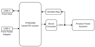
The USB-C port dedicated to connection to a Host PC can sink and source power as well as handle USB2 data communication.  The second Port is to only receive power.

How can I simulate our PD requirements with the TPS65988DKEVM?  The EVM should be able to do everything but supply a voltage to the Host exceeding the voltage received on the "From Power Adapter" port.

Please provide me with EVM jumper settings as well as a sample .prj file that I could use to start with to modify for our requirements.

Thanks,

David 

  • Hello David, 

    I am currently looking into creating and testing a sample project (.pjt) file. I will confirm the EVM jumper settings as well and get back to you as soon as possible. 

    Best,

    James

  • Thanks so much. Will I need to use external switches for both ports or is it possible to use the internal switch for the port that only receives power?

  • Hey David,

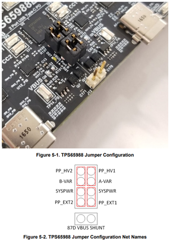
    Out of the box, the TPS65988EVM has jumper configuration for a TPS65988 device. With this configuration, the two internal power paths are configured as Source paths for their respective Type-C ports. The two external power paths are configured as Sink paths for their respective Type-C ports.

    I will refer to your "from Host" port as "port A" & "from Power Adapter" port as "port B"

    Since port A is for both source and sink it will require both the internal switch and external switch to test for DRP (Dual Role Port) capabilities on the EVM.

    Since port B is sink only, you have the choice to use either the internal or external power path. Whatever you choose, you will reconfigure it via the project file to work as a sink path.

    Additionally, the default jumper settings will be sufficient for your initial testing. This information is on Page 7 of the attached document. 

     TPS65988 Evaluation Module.pdf

    Hope this helps! 

    Best,

    James 

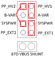
  • I have tried to make things work with Port B using the internal path for the sink path.  I set the jumpers as follows:

    I have not been able to get things to work like this.  I would like to use the PD controller this way since it requires less circuitry.  I would like to not include the external switch on Port B if possible.

    Best regards,

    David

  • Can you provide a .prj that would work for these Jumper settings?  I have already had an E2E thread where in the end the .prj did not work.  in the .prj that I was provided, both the internal and external switches were activated when connected to Port A. 

  • Hi David, 

    Can you provide the previous .pjt file that did not work on your end? 

    Thanks and Regards,

    Raymond Lin

  • I altered the Jumpers as follows:

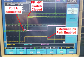
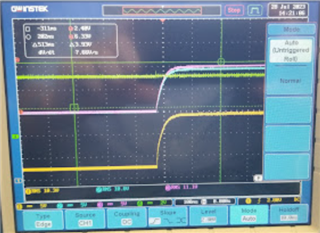
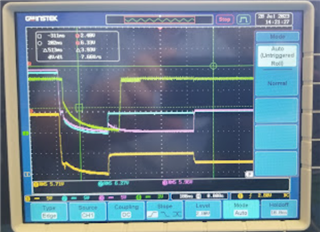
    Then when looking at signals found this:

    Green: PP_HV1

    Yellow: External P-Mosfet Gate Voltage

    Blue: Common P-MOS Source voltage

    Pink: SYSPWR

    This is what happens with Port A is connected to NB:

    This is what happens when the USB charger is plugged in to Port B

    This is what happens when the charger is disconnected from Port B

  • Hi David, 

    We're working on providing a sample pjt to test out the basic requirements you laid out. 

    Regarding the usage of the internal power path, the EVM was designed to use the internal paths (labeled as PP1 and PP3 in the GUI for Port 1 and Port 2 respectively) as source paths while the external paths (PP2 and PP4 for Port 1 and Port 2 respectively) were designed for sink paths. We're looking into if it's possible to use the internal paths for sink since these are directly connected to DCDC on the system side (LM3489 to be exact). 

    Thanks and Regards,

    Raymond Lin

  • "We're looking into if it's possible to use the internal paths for sink since these are directly connected to DCDC on the system side (LM3489 to be exact)."

    My understanding is that this should be altered with the jumpers- Correct?

  • Hi David, 

    Yes, that is correct. This can be altered with the jumper settings you have configured.

    The project file configuration must match the jumper settings above in order for this to work on the EVM. I have a working project file configured so that Port A (Port1) is source-only (PP_HV1/PP1) and Port B (Port 2) is sink-only (PPHV2/PP2). I understand that your application requires port A to be DRP (both source and sink). I will test on my end and provide you with a project file for your specific application.

    For now, please do let me know if you are able to source with Port A and sink with Port B. 

    Best Regards, 

    Aya

     TPS65988DK_PortA_Src_PortB_Snk.pjt

  • Thanks Aya,

    Here is my progress

    1. Connect Port B to charger

    2. Connect Port A to Laptop

     result: I can source with Port A (19.2V, current draw 1700mA) and sink with Port B (20V)

    Everything looked OK on my PD analyser.

    Next test:

    1. Connect Port B to charger

    2. Connect Port A to Samsung S8 cell phone

    result:  Sourcing on Port A would re-try things over and over.  

    The screen of the PD analyser would fill up VBUS would 

    I had a load resistor on the SYSPWR to GND for testing.  Unfortunately when probing things, I bumped the resistor lead and shorted SYSPWR to GND.  After this, the board will only source a max of 5V to the laptop onj Port B.  Prior to this, the analyser showed it would source 19.2V.  

    I need a new EVM.  Did you try the project file on an EVM?  

    I have had quite the time with mine.  The only EVM available was a TPS65988DJEVM.  I ordered this and asked about how to get things to work with my application on E2E.  I was told that I could not use this since it was the DJ version.  I wasn't able to find availability of the DK version so asked if I swapped out the TPS65988DJ with the TPS65988DK if this would work.  I was told yes.  We had a contract SMT house swap it.  It did not work.  I found bad solder joints.  I fixed this but have not been able to get things to work- I am was not convinced that it was the project file or if there were hardware problems before, but now    I have definitely now damaged the board.

    I would like to order a new TPS65988DKEVM but have not been able to do so on the TI web site or anywhere else.  When I press the REQUEST button 

    www.ti.com/.../TPS65988DKEVM

    I am then directed  a form that looks like it has to do with requesting software.  I have now filled this out twice and have not gotten any response that would lead me to being able to order an EVM.

    More details on our requirements:  

    Our system requires 35W of power maximum.  If less than that is available, product functions are limited (which is OK for this product).  Any excess power received on Port B will be offered back to Port A.

    Are you able to create a .prj file with the jumpers on your EVM set as we have determined is necessary and demonstrate that my requirements can be met?  If you can do this, then I should be OK.

    David.


  • Hi David, 

    1- For your first test, it seems everything worked as expected. Port A was sourcing and Port B is sinking as configured both in the GUI and jumpers. 

    2- I was able to achieve your initial requirements: Port A --> DRP (Source and Sink) Port B--> Sink-only using the internal power paths only. I tested the project file below with a TPS65988DK EVM along with a DUO-board for all 3 scenarios above, and the behavior was as expected in terms of the power negotiation ( I did not test data capabilities on Port A but there should not be an issue with this, just wanted to make sure we have the power aspect first).

    The jumper settings remain the same in terms of our previous discussion:

    See project file for this working case below:

     TPS65988DK_PortA_DRP_PortB_Sink.pjt

    3- I'm sorry to hear the EVM has been damaged. I will reach out to one of our experts to see if there is something you can do to repair it. Also, I will check to see the current availability status of the TPS65988DK EVM and get back to you on that. 

    For now, I hope you have the assurance that your project design requirements are met using a TPS65988DK EVM. Please let me know if you have additional questions/concerns. 

    Best Regards, 

    Aya

  • Thanks so much Aya! Great to hear that you were able to my the initial requirements met! I suspect that I may have had damage to my board even before last night.

    Ok to not ask about having the board repaired.

    I am reasonably confident that I can go ahead with schematics and not spend any more time with the EVM (I have learned a lot but unfortunately it was the hard way :-)) . 

    I have a question regard the TPS65988DK_PortA_DRP_PortB_Sink.prj project file.  

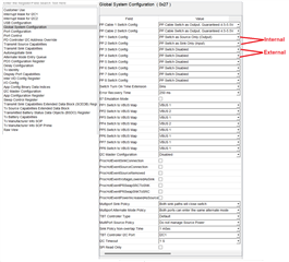
    My understanding is that the internal and external switches are assigned on the page as shown below.  Is this correct?  Are PP1-PP4 for internal and external paths as I  understand?

    My understanding is that PP3 Switch Config would need to be assigned as a Sink Only (Input).  How can it work if it is set as "PP Switch Disabled"?

    David

  • Hi David, 

    No problem!

    Yes, that is correct. PP1 (PP_HV1) and PP2 (PP_HV2) are the internal power paths. PP3 (PP_EXT1) and PP4 (PP_EXT2) are the external power paths. 

    The two internal high-voltage power paths are bi-directional, and can be used as either a sink or source, or both. There is a setting in the GUI to change PP1 to " PP Switch as Sink or Source". You do not need to use the external power path. 

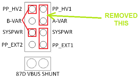
    I removed the jumper cable that is connecting PP3 and the behavior remains the same. 

    Best Regards, 

    Aya