Hi,
I am reviewing the timing diagram provided in the datasheet,
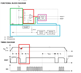
I noticed that it only includes timing information for reset triggered by power-up and reset triggered by WDI. There's no information about the MR (Master Reset) aspect.
However, upon examining the BLOCK DIAGRAM, I noticed that this RESET IC has these three triggering mechanisms, all of which send a signal to the RESET LOGIC BLOCK.
When looking at the circuit triggered by voltage changes that result in a reset, it appears to be a comparator circuit. Based on the timing, when the voltage drops (leading to a LOW output from the operational amplifier, OP), it triggers the RESET circuit within the RESET LOGIC, resulting in a RESET output.
Yet, as indicated by the red circles in the timing diagram, the voltage quickly rises back to its normal level, causing the OP output to become HIGH again.
The signal input to the RESET LOGIC, transitioning from LOW to HIGH, is actually very brief.
However, the RESET output remains active for a fixed duration of ( T? + Td )time.
Does this imply that when the RESET LOGIC circuit triggers the RESET output action, the operation of the RESET LOGIC BLOCK won't be influenced by changes in external MR signals? Regardless of how the input to the MR pin changes, it will always complete a fixed RESET timing.
From the current understanding of the RESET timing due to voltage changes, it seems to work like this.
Or is it possible that when the RESET FUNCTION is activated, the state of the MR pin still affects the RESET output? For instance, if the MR signal is pulled HIGH before the RESET signal has completed the Td time, does this affect the reset process?