Hi
I'm designing a battery charger with the TPS55289.
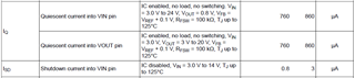
The datasheet provides some information about the quiescent current into Vout:
Quiescent current into VOUT pin
IC enabled, no load, no switching, VIN
= 3.0 V, VOUT = 3 V to 20 V, VFB =
VREF + 0.1 V, RFSW = 100 kΩ, TJ up to
125°C
760-860 μA
- I take it "IC enabled, no load, no switching" means that the Mode register, OE field is set to "Output disabled"?
- Does pulling EN Pin low influence the quiescent current into Vout? If so, how large is Iq when the IC is not enabled?
Your help is appreciated.
Tobias