This thread has been locked.

If you have a related question, please click the "Ask a related question" button in the top right corner. The newly created question will be automatically linked to this question.

LM5122-Q1: Two-phase boost converter has one phase (the slave) for which the high-side device (HO) stops switching as the output current increases.

Part Number: LM5122-Q1
Other Parts Discussed in Thread: LM5122, LM5122EVM-2PH, LM5122ZA

Hi TI Team, 

We have designed and built a two-phase boost converter with the following operational parameters:

  • Vin = 36-53VDC (48VDC Nominal)
  • Vout = 60VDC
  • Pout(continuous) = 250W
  • Pout (100ms) ≥1kW

I'm able to share schematics/layout privately, as covered by our MNDA on file. Please let me know where I should send. 

Our issue is that the slave device begins, around 10A of output current, to intermittently drop pulses. As we increase the current, it drops out entirely.

We checked the feedback loop and the components are correct. We also looked and saw that the timer cap is not being discharged (as would be the case in a hiccup mode event). Even so, we grounded the RES net shared between the two devices just to check, but the issue remained. Finally, we swapped out the part, and it the issue persisted.

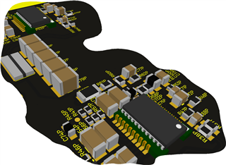
One thing we noticed about the layout is that there was a polygon that was intended to connect the PGND pins on the 5122 back to the EP pad under the part (to join the AGND pin) and, for some reason, this was missing. They are missing on both the Master and the Slave devices, but the slave device is having the issue. We attempted to bring the AGND and the PGND together by placing a large shorting wire over top of the device. We then grounded that shorting wire to an adjacent ground plane.

We are also attempting to measure the LO output signal and noticing that the signal does not appear to be pulling down to ground (it's relatively constant across load- pulling down to 1-2VDC. This makes us wonder if the dead time block inside the IC is preventing the high side from turning on.

We've noticed a few other e2e posts in which other engineers were having issue with the slave controller's high-side device dropping out under increasingly heavy load, so we're wondering if there is a particular susceptibility to this phenomenon for a device operating as a slave device.

  • HI,

    thank you for using the E2E forum.
    You can share the schematic via private email - just click on my name an selected private email.

    Once done, please drop here a not as well.

    Best regards,

     Stefan

  • Stefan,

    I did not see an email via the E2E system. I did, however, send you a private message requesting your email address. Would appreciate it if we could get it to you today for review – we are currently blocked on proto delivery to the client and, after several attempts, most of our troubleshooting seems to indicate a higher susceptibility to noise for the controller when used in slave mode.

    Can you tell me what is the maximum slew rate for the gate drive outputs? Also, could you tell me which blocks inside the part (besides the dead time block could cause the high side driver to begin to drop pulses?

  • Hi,

    so far I have not received and data - but please note for a schematic and layout review we need typically 2-3 days.

    Best regards,

     Stefan

  • Hi,

    can you please try to generate a layout image which has the routing and the component designator in one image.

    The the provided files the review is a huge effort to sort out what is placed where and how it is connected.

    Best regards,

     Stefan

  • Hi Stefan, I just responded in private message and included the outer layers with a silk screen for you. Hopefully that will give you what you need.

    One thing to note was that we were able to increase the threshold at which the high side device began to drop out by slowing down the gate with a more aggressive snubber. What is the maximum DV/DT for the LM5122?  It is starting to look like the LM5122 has a maximum DV/DT that is lower than the speed at which we are moving.

  • One other point of reference is an E2E post that we found that seems to be related. 

    Maybe this jitter issue is related. Have you seen any instances in which providing an external sync clock fixed this issue?

  • Hi Cody,

    Did you receive any update from our side?
    If not, could you send the details you prepared for Stefan to me as well?
    Feel free to send them via private message if you cannot disclose them here in the open forum.

    Thanks and best regards,
    Niklas

  • We have not, unfortunately. We are really stuck on this issue- and all things are starting to point to an undisclosed issue with the IC when used in slave mode. I will send you a private message.

  • Hi Cody,

    Thanks for reaching out to us via e2e.

    It is a bank holiday today. Please expect a response by Wednesday.

    Best regards,

    Feng Ji

  • Stefan? Niklas? Feng? Any update here?

  • Hi Cody,

    Sorry for the long delay.
    I received your message including the schematic and layout files.

    Like you already mentioned yourself, separating AGND and PGND can have negative effects on the device, like the two ground floating away from each other.
    Has there been any improvements of the behavior after the two GNDs have been connected artificially?
    I also noticed on the layout file, that the design uses thermal relieve pads, which makes it easy for soldering but can have negative impact on performance, thermal behavior and stability.

    Both LM5122 device work fine at lower loads and do only show abnormal behavior on the secondary device at high loads, correct?
    Do you have waveform measurements during operation, that show the switch node of the failing device?
    I would also be interested if one of the devices enters an overcurrent state, with the voltage at the current sense pin goes above the threshold.

    Best regards,
    Niklas

  • Hi Niklas,

    Thank you for responding. Here are the answers to your questions:

    Has there been any improvements of the behavior after the two GNDs have been connected artificially?

    No, we hard tied both of them with a large gauge solid conductor and it had no effect.

    I also noticed on the layout file, that the design uses thermal relieve pads, which makes it easy for soldering but can have negative impact on performance, thermal behavior and stability.

    The thermal reliefs were a little over aggressive and will be minimized on the next build.

    Both LM5122 device work fine at lower loads and do only show abnormal behavior on the secondary device at high loads, correct?

    The master device is rock solid up to even high currents. The slew rate in that device can reach 12V/ns with no issue. The slave device begins to drop high-side pulses around 7V/ns.

    I would also be interested if one of the devices enters an overcurrent state, with the voltage at the current sense pin goes above the threshold.

    Neither device is near the current limit. In fact, we are able to able to swap the 3mOhm sense resistor with a 5mOhm resistor in the master device and make nearly 2x the slave current without dropping any pulses. 

    We have tied Res pin hard to ground for both devices to avoid hiccup mode as well. We've tried clocking the two devices externally, we've filtered the Voltage that feeds the FB pin.

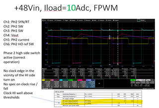
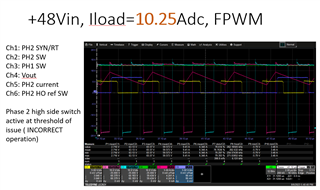
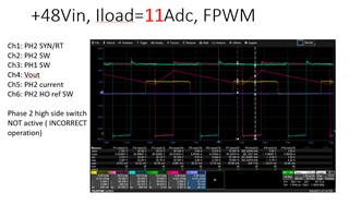
    Screen shots are below:

    Correct Operation:


    High-side beginning to drop pulses:

    High-Side inactive:


  • For what it's worth, there are other folks who seem to be having the same problem with this device:

    https://e2e.ti.com/support/power-management-group/power-management/f/power-management-forum/545659/lm5122-2-phase-waveform-jitter-on-slave-chip---master-ok?tisearch=e2e-sitesearch&keymatch=LM5122%252520jitter

    From above:

    "Because the TI LM5122EVM-2PH exhibits the same problem with jitter on Phase 2 (slave), I would be satisfied if you could obtain one of these boards and observe the phase 2 waveform yourself. We have tested it at half load and at full load. The EVM has a fixed 28V output with a 9V-20V input range. It exhibits the jitter only on Phase 2 (slave) at an input around 12-13V. The EVM has essentially the same synchronization circuit as ours does, which is traceable back to the LM5122 data sheet. I am focusing on the slave phase jitter and not the phase current imbalance. I am confident we can fix the current imbalance ourselves once the jitter problem is fixed. We need to be certain that the LM5122 does not have some inherent problems. At this point we believe it does. Both phases operate at the same frequency both on your design and ours."


    https://e2e.ti.com/support/power-management-group/power-management/f/power-management-forum/873392/lm5122-slave-jitter-in-interleaved-mode?tisearch=e2e-sitesearch&keymatch=LM5122%20%22slave%20jitter%20in%20interleaved%20mode%22#

    Can you please see if you can replicate this on your EVM? 

  • Hi Cody,

    I made some internal research on this and similar issues with LM5122 and found out the following:

    This seems to be a know issue with the device, which only occurs with multi phase systems under high load conditions.
    There is an alternative version LM5122ZA: https://www.ti.com/product/de-de/LM5122ZA
    This device has this error fixed due to internal layout adjustments.
    However, this device is only P2P with LM5122Z package (24 pins). The non-Z package only has 20 pins, therefore a re-layout would be necessary to use the ZA version.

    Other customers were also successful in improving the skipped pulses by increasing the gate resistance of the low side FET.
    This design seems to use GaN FETs, so I am not sure if the same approach is effective here.

    Best regards,
    Niklas

  • Hi Niklas, 

    Thank you for very much for chasing this down for us- this information is extremely helpful. We are making an interposer board that will allow us to put the 24pin on the 20pin footprint. One question I do have is whether you think there would be any reason that we would need to change both the master and the slave device? We're thinking of only changing the slave device out on the existing boards (with ground tie fixes implemented) to see if it allows us to achieve normal operation.

    We'll have to trim the leads and hand form them to get the new part to solder down to the interposer board, but it sure bits inserting even more delay in the schedule for a board spin before being able to delivery the proof-of-concept prototypes to the client. 
    If anybody happens upon this issue in the future, we'll likely have a stock pile of these interposer boards for sale, since minimum buy is fairly high.

  • Hi Cody,

    Thanks for the update.
    If the primary (20 pin) device works without issues, I see no need in changing both ICs. There should be no problem in combining the primary 20 pin device with the replaced LM5122ZA device on the secondary phase.

    There will be updates on the LM5122 device with this issue, so feel free to stay in contact with our FAEs and marketing contacts to stay up to date.

    Best regards,
    Niklas