This thread has been locked.

If you have a related question, please click the "Ask a related question" button in the top right corner. The newly created question will be automatically linked to this question.

TPS53015: Start up failure with pre powered pull-up

Part Number: TPS53015

Hello TI team,

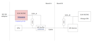
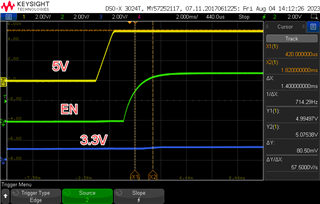
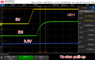
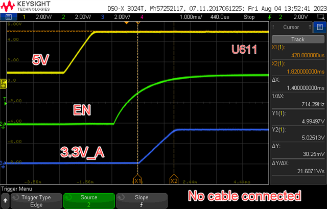
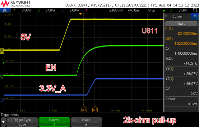
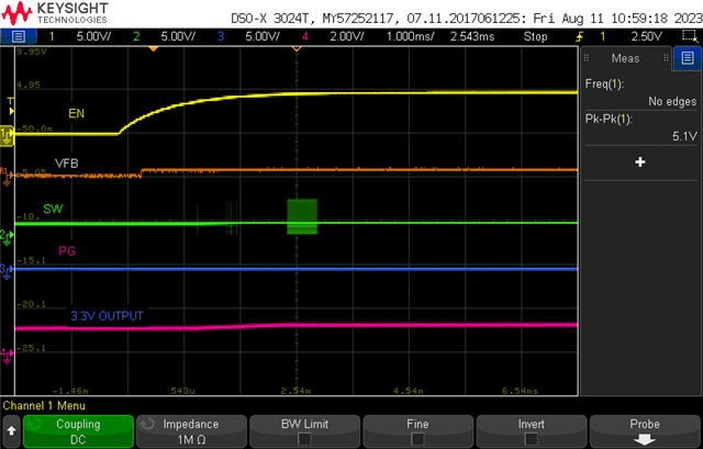
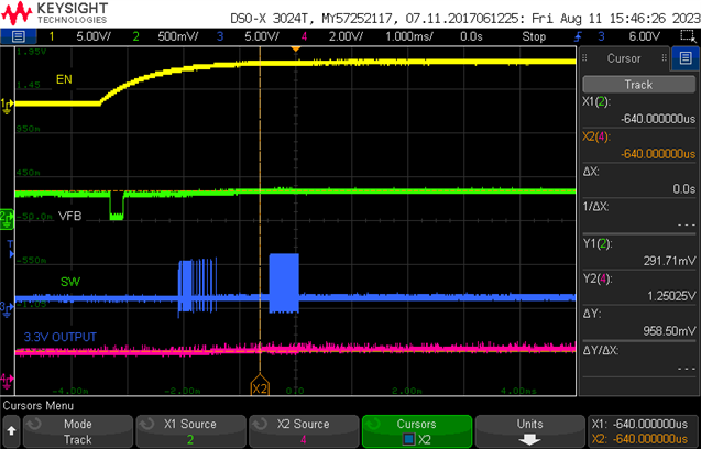
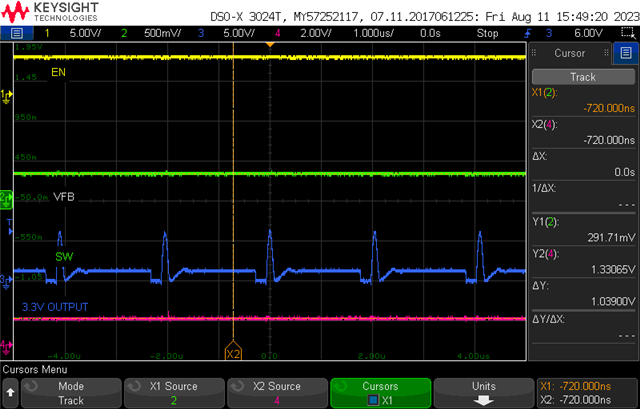
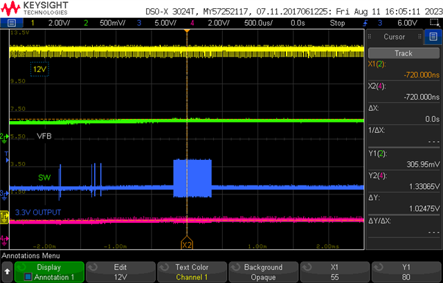
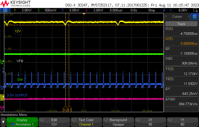
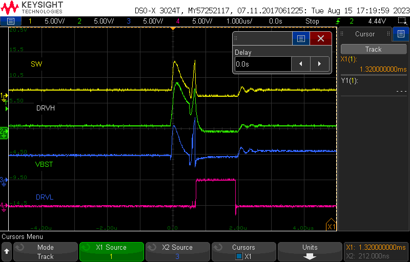
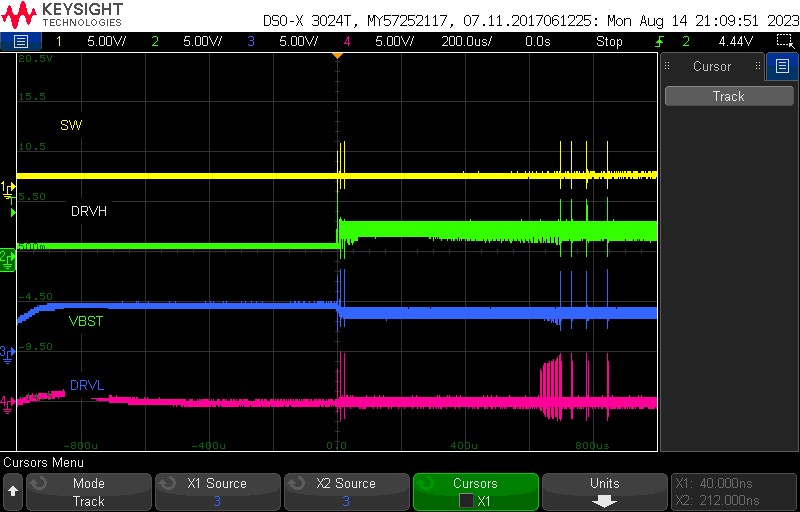
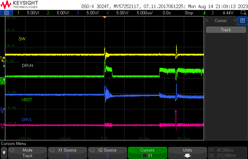
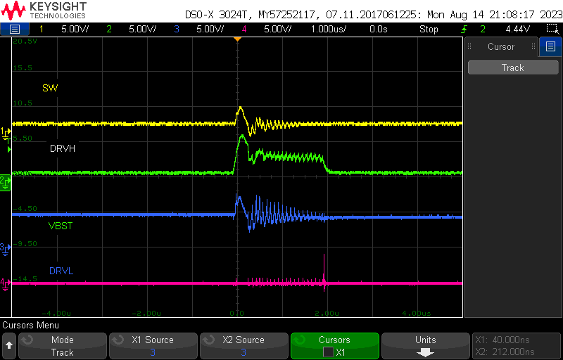
The 3.3v DC/DC doesn't start properly as shown in the capture, it stays around 1.2V.

Can you confirm this is is an expected result?

3.3V_B is always on as long as DC_12V is plugged in, and 3.3V_A is turned on when the power button is pressed.

Thank you!

Choon

  • Choon,

    Is the 3.3V waveform taken at the output of the TPS53015 (3.3V_A node)? We will need to review your schematic to determine if the device has been configured correctly. Please attach for further review. Thanks

    Best regards,

    Britton

  • Hi Britton,

    Yes, 3.3V was measured at 3.3V_A, TPS53015 output.

    Please find the attached schematic.

    Thanks,

    Choon

    DC_3P3V_TPS53015.pdf

  • Choon, 

    We will get back to you tomorrow after reviewing. 

    Thanks,

    Britton

  • Hi Choon, 

    We reviewed the schematic and do not think the behavior is expected. I have a few questions:

    1. How is 1.2V being applied to the output rail? 

    2. Is the behavior different when the output is not prepowered?

    3. Can you capture waveforms of the SW signal, PG signal, and VFB signal, before during and after soft start?

    These will help us out with our debug.

    Best regards,
    Britton

  • Hi Britton,

    1. How is 1.2V being applied to the output rail? 

    > It stays at 1.2V level all the time since the board-A power is on.

    > FYI, it's back powered from 3.3V_B pull-up through the cable. The 1.2V is not applied if the cable is disconnected, and it starts normally without any errors. *** It also starts normally when the pull-up resistor value is 2kΩ instead of 1kΩ at Board-B.

    2. Is the behavior different when the output is not prepowered?

    > It's completely normal start-up as below waveform.

    3. Can you capture waveforms of the SW signal, PG signal, and VFB signal, before during and after soft start?

    > I'll capture and upload very soon.

    Thanks,

    Choon

  • Hi Britton,

    This is the capture of SW, PG and VFB with EN and 3.3v_output.

    Thanks,

    Choon

  • Hi Choon,

    I will take a look at this Monday and get back to you while Britton is out of office.

    Thanks,

    Joseph

  •  

    Britton is out of the office for a few days and asked me to assist you:

    I can't read the value on the voltage of the FB pin, but it looks like it comes up when EN comes up, and then there is some switching activity at about 2.5ms after EN comes up, then it suddenly stops.  That timing seems really close to the UVP enable delay at the end of Soft-Start.

    Would it be possible to trigger on the switching node using the "Normal" triggering setting rather than "auto" and trigger on the switching node at 6V, and zoom into the waveform so we can see the switching more clearly?

    Also, can we check what the FB voltage is in these waveforms?  with 1.2V on the output, FB should be 0.25V, but I can't tell if that is what you are reading on FB or not.

    Also, can you try removing the C12 feed-forward capacitor?

  • Additionally, the Ceramic input capacitance on this design - 2x 1.0μF with a 22μF electrolytic capacitor seems small.  Have you measured the Drain voltage on Q1A (Pin 7 and 8) to make sure the input voltage to the converter isn't falling excessively when switching starts?  A quick calculation suggests we should see about 200mV drop on VIN during the initial on-time pulses at 12V to 1.2V, if with DC bias derating of those capacitors, we might be seeing more.

  • I captures SW and VFB again using 6V trigger at SW node and zoomed in as well.

    As shown on the capture, FB voltage is 0.291V@3.3v=1.25V roughly.

    I tried removing the C12 feed-forward capacitor but there's no change at the start-up waveform.

  • I captured 12V input during start-up, it's pretty noisy about 640mV level peak-to-peak that comes from the 5V DC/DC right next to it. But I couldn't see a voltage deep for 12V, I think the reason is that additional 63uF ceramic and 33 tantalum capacitors are at the 2V line for other circuits.

    Do you think we should clean up the 12v noise to get the proper 3.3v start-up?

  •  

    The Switching Node waveforms don't look right, like the high-side FET is not getting turned on.  It looks like the voltage is only getting to about 6V when it should be getting to 12V.

    Check the values of R1 and C4, and check the VBST voltage waveform on pin 10 of the TPS53015.  Also check the DRVH (Pin 9) voltage.  It should be pulled up to about 17V during the high-side ON time and down to 5V during the low-side MOSFET on-time.  If R1, which is suppose to be 1Ω is too large or C4 too small, the high-side Driver wont have enough charge to turn-on the high-side FET during the ON time.

    With the switching node sitting at 1.2V when the low-side FET is off, here might not be enough charge on C4 if R1 isn't allowing C4 to charge during the off-time.

    If R1 and C4 both check out, but DRVH is still not pulling up to 17V, we could try adding a diode from Vreg (Pin 3) to the junction between R1 and C4 to recharge C4 more quickly.

  • I measured R1 and C4 values, and they are correct as in the schematic, R1=1Ω, C4=0.1uF.

    I changed to 0Ω on R1 but it didn't affect the waveform. I also tried 0.47uF on C4 but the DC/DC still failed.

    After adding a diode between VREG5 and the R1/C1 node, I finally captured a decent starting waveform as shown below.

    I believe the pre-powered pull-up resistor prevented the bootstrap capacitor from recharging.

    Anyway I really appreciate your detailed help!

  • The waveforms below are SW, DRVH, DRVL, VBST failing to start.

  •  

    I'm glad we were able to help you and address the issue.  If you have any other questions, please create a new thread so we can assign it to the correct person for support.