This thread has been locked.

If you have a related question, please click the "Ask a related question" button in the top right corner. The newly created question will be automatically linked to this question.

LM5176: 4 switch BUCK converter MOSFET getting heated

Part Number: LM5176

Hi Team,

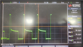
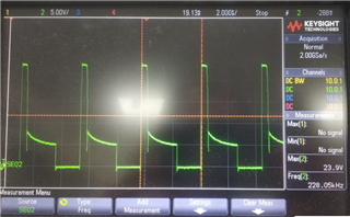
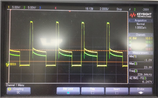
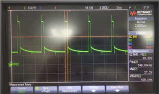
We have the Buck converter prototype board using LM5176, input voltage 24V and output 5V. while power ON the board we got the 5V output voltage without connecting any load .

But we have noticed that first MOSFET Q1 getting heating up and 24V input side drawing current almost 250mA.

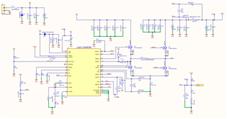
Kindly find the below picture of reference schematic and let us know any update required in schematic or your suggestion to solve this issue. 

  • Hi Shinod,

    thank you for using the E2E forum.

    Can you probe the HDR1 and SW1 and send the scope plot?

    How does the design behave under load?

    Is the output voltage stable - please probe this as well.

    Best regards,

     Stefan

  • Hi Please find below the HDR1 and SW1 and 3rd is both complained screen shorts respectively. HDRV1 is not going down in OFF time almost 2V higher compare to SW1

  • Hi Shinod,

    i assume - please confirm.

    channel 1: HDRV

    channel 2: SW1

    The Buck highside FET Gate is referenced to SW1.
    So to open the MOSFET the Gate signal needs to be above SW1 with the at least gate threshold.

    So it looks like this MOSFET does not get a proper signal. 

    Please also check the BOOT1 voltage.

    Best regards,

     Stefan

  • Hi Stefan, MOSFET ON signal seems proper  because we are getting 27V (t= 438nS). but I worried MOSFET OFF time during the OFF time we are getting 2V higher compared to SW1. kindly find below the Boot1 wave form for your reference looks ON time voltage is good (27V) for 22V input). Only Q1 is getting heated because of this Buck converter is loading at 250mA input current. Request you to verify schematic and components value, also Gaudi me why this issue ?

  • Hi Shinod,

    According to the datasheet, LM5176 runs in CCM operation. This allows negative currents through the inductor at light loads, which can drastically reduce efficiency for a more stable output voltage signal.

    For a general review of the schematic, could you please fill in the quickstart calculator tool for LM5176?
    https://www.ti.com/tool/download/SNVC208

    Thanks and best regards,
    Niklas

  • Hi Niklas,

    we are using this LM5176 for USB PD 140W product along with CYPD3175, But initial stage we should get 5V by default, we got 5V output but MOSFET Q1heated up so we got stuck. Our PD profile is (5V/3A, 9V/3A, 15V/3A, 20V/5A, 28V/5A) once default 5V is fine PD controller will adjust the Feedback voltage and set the required voltage. find the attached file of LM5176 quick start tool for schematic review. If Q1 gate driver is not proper, how to solve that issue. 

     LM5176 Buck-Boost Quickstart Tool.xlsm

  • Hi Shinod,

    Thanks for filling in the calculator.
    I will review the design and get back to you within 1-2 days.
    Thanks and best regards,
    Niklas

  • Hi Shinod,

    Sorry for the long delay and the e2e maintenance off-time.

    - The inductance used for this design is rather load. This lead to larger current ripple, which increases stress on the inductor and FETs.
    For this design, I would recommend to increase the inductance to at least 15uH.

    - The compensation might be improved as well. This would not affect DCM operation, but as the device is running in CCM permanent, it can improve the light load behavior as well. I would recommend to have at least 60 degree phase margin.

    If there is no change visible after making improvements here, we might also take a look at the layout.

    One more general question from my side:
    For Vin 23V-32V and Vout 5V, a buck-boost topology was chosen. Was there a reason you did not choose a pure Buck topology?

    Thanks and best regards,
    Niklas

  • Hi Niklas,

    Thanks for your feedback,

    As I mentioned above our actual use is USB type C PD 140W application with CYPD3175 PD controller chip. So we need 5 level of output voltage like 5V, 9V, 15V, 20V and 28V, from 24V or 32V input supply. but now I can fix only 24V input. PD controller FB pin will be connected to LM5176 FB pin to control the FB voltage to get different voltage level, LM5176 default voltage is 5V. here 28V output LM5176 shall act as boost converter.

    So we have calculated inductance value for 28V output its shows 4.7uH only, Let us know for all five level of voltage (5, 9, 15, 20, and 28) what inductor value is best.

  • Hi Shinod,

    Thank you for the clarification. This makes more sense to me now.
    In this case, I would recommend checking the worst case conditions with Vout min and Vout max and select a inductor and compensation that is still stable under all scenarios.

    This can be done with the calculator as well.
    For additional resource, we also have the power stage designer tool, which shows inductance recommendations and ripple currents graphically.
    https://www.ti.com/tool/POWERSTAGE-DESIGNER
    It does only support Buck and Boost as separate topologies, but the calculations are universal.

    Best regards,
    Niklas