This thread has been locked.

If you have a related question, please click the "Ask a related question" button in the top right corner. The newly created question will be automatically linked to this question.

BQ77915: Stacked Design

Part Number: BQ77915

Hey Guys,

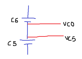
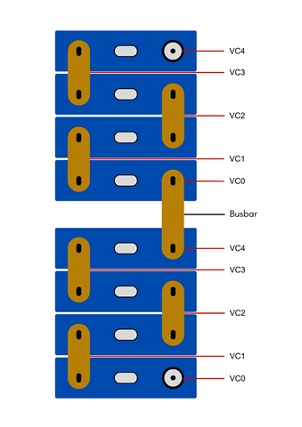
I've attached the schematic for a 16S Design

can you please review it ?

Do let me know if any improvements can be made for additional safety 

Thanks & Regards,

Muki

Schematic V5.1

  • Hi Muki,

    Your schematic looks good, the only change to make is at D25.

    As it is, the diode bypasses the MOSFETs and makes the CHG protections obsolete. You will need to either remove it or add another diode back-to-back with it so that the FETs are not bypassed.

    Regards,

    Max Verboncoeur

  • Hey Max,

    Thanks for the quick review

    I've replaced D25 with a new diode, pls let me know if that works

    1. should i also replace D23 with the new diode ?

    2. what voltage rating should i choose for C1 to C28 and C29, C30, C34, C35 ?

    Regards,

    Muki

  • Hi Muki,

    The new diode should fix the problem.

    D23 should be fine as is. 

    The voltage rating for your capacitors should be greater than what voltage you expect to see across them. For the capacitors parallel to the cells, that would be the individual cell voltage. For the capacitors between AVDD/VDD and VSS that would be the stack voltage of all the cells on that device. For C34 and C35, you'll want that to exceed the voltage of the entire stack, as when a load is present and the protections are enabled, Pack- can be pulled up to Pack+. C29 and C30 should also exceed the entire stack voltage.

    Regards,

    Max Verboncoeur

  • Hey Max,

    Appreciate the detailed explanation

    Schematic V5.3

    I've attached the schematics for a secondary protector. The fuse I'm using doesn't have a heater and needs high current to rupture. So, i'm testing multiple FETs in parallel for blowing the fuse.

    Pls take a look at the designs and let me know :

    1. if i need R19 as an additional resistor (or) if i could just use FETs in parallel as shown in sheet 2/2. Is there even any difference between them ?

    Regards,

    Muki

  • Hi Muki,

    R19 would be redundant. What you're doing is putting R19 and R18 in parallel, it is equivalent to placing a single 500kohm resistor in place of the two.

    Go with the schematic shown in sheet 2, everything else looks correct.

    Regards,

    Max Verboncoeur

  • Hey Max,

    I went through the layout guidelines for stacking BQ77915

    It says that the trace connecting the VC5 of a lower device to the cell should be separate from the trace connecting VC0 of the immediately upper device to the next cell

    Based on this, I've changed the connector configuration

    Pls advice which would be better for the device's performance, the new design or the previous one

    Schematic V6.1

    Regards,

    Muki

  • Hi Muki,

    What this guideline is referring to is the PCB layout. Your schematic will not reflect this, and you should add back the connections between each VDD and the above VSS.

    The guideline is saying that on the PCB layout VC5 and the above VC0 should have their own dedicated trace to the cell. See the image below. The red lines are the traces that you'll want for these cell connections, they're still electrically connected, which is why you won't want to alter your schematic, but they split into their own traces as soon as possible.

    Regards,

    Max Verboncoeur

  • Hey Max,

    Need a little clarification

    they split into their own traces as soon as possible

    If this is the case, then the new design makes more sense. VC0 and VC4 traces will be split closest to the cell connection.

    you should add back the connections between each VDD and the above VSS

    They may not be connected in the PCB but they will still be electrically connected through the busbar

    I understand if this won't work, I'm just curious as to why

    Regards,

    Muki

  • Hi Muki,

    If they're electrically connected as you've indicated, then there is no issue. I recommended adding the connections back to the schematic so that it is clear that they are connected, however it is not necessary to do so.

    Regards,

    Max Verboncoeur