


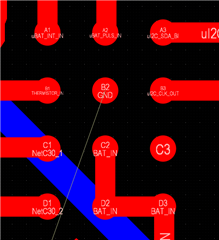
The B2 and C2 pins are trapped in the BGA package. For C2 I can parallel it with D2 to get it attached (but this contravenes the routing guidelines shown in the datasheet). However I cannot get B2 out.
The demo board guide seems to show using holes for this BGA pads. However, I can't find any TI recommended footprints/recommendations for pulling GND out. Are there any recommendations for this (hole/pad size/solder mask relief etc)?
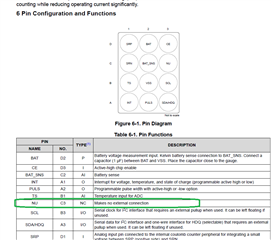
Another option MIGHT be to use the "NU" pn (C3) to connect into GND. The datasheet shows that this is not externally connected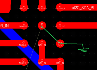
There might be other options I am unaware of. Any help would be appreciated.
