This thread has been locked.
If you have a related question, please click the "Ask a related question" button in the top right corner. The newly created question will be automatically linked to this question.
Hello, TI:
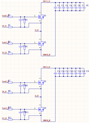
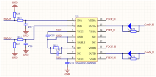
I use UCC21542 to drive a half bridge module, of which the schematics are presented at the end. Each arm of the bridge consists of two MOSFETs in parallel. The auxiliary power supply for each arm is 15V (isolated). A zener diode is used to generate +12V/-3V for the gate driver. That means VDD is 12V, VSS is -3V.
The MOSFET is NVH4L040N65S3F, the datasheet is attached.0815.MOSFET.pdf
1) The Qg_total of each mosfet is 160nc@10V. The switching frequency is 50kHz. So, the total power consumption to charge and discharge the mosfet is approximately 2*160e-9*1.5*15*50e3*2 = 0.72W. Is it correct? The external capactor between G-S is 100pF, which is ignorable.
2) The gate resistors consist of two parts: two separate 1Ω resistor are placed at the G terminal and S terminal of each mosfet; a common 1Ω resistor acts as another turn-on resistor while the diode is used to reduce the turn-off resistor. In this way, if the two MOSFETs are equalized as one, the equivalent turn-on resistor is 2Ω, while the turn-off resistor is 1Ω.
3) The internal gate resistor of each mosfet is 1.9Ω. Therefore, the equivalent internal gate-resistor is 0.95Ω.
4) I am somehow confused by the equations to calculate the power consumption of UCC21542, as provided by its datasheet. I guess the power consumption of UCC21542 should not have exceeded its limit.
However, when the DC-link bus voltage is increased to 150V while the load current is 30A DC. The UCC21542 is damaged but the MOSFETs are OK.
Could you please help to address my questions?
1) What is the most possible reason for the damage of UCC21542?
2) Does the power consumption exceed the limit of UCC21542?
3) Is it right to place resistors at both the G terminal and S terminal? I thought this should be necessary for paralleling two MOSFETs.
4) I will try to increase the external turn-on resistor, but I am not sure if this is the right solution.
Thanks and best regards.
Hi Jiaxing,
1. The power should be Qg*Vgs*fsw. Based on Figure 7 in the NVH4L040N65S3F datasheet, 160*1.5 sounds a little high for the gate charge. But 160n*1.5*15V*50kHz is only 180mW. I don't see where the additional 2*2 enters the equation.
2. The most probable cause of damage is switch node ringing and a transient overvoltage on the supply, which is unrelated to power consumption. Do you have waveforms from your testing of the output voltage and the switch node voltage?
Your circuit schematic should work, but you might have to add protection diodes and improve the layout.
Best regards,
Sean
Hi, Sean, thanks very much for your reply.
1) Because 2 MOSFETs are used in parallel. Besides, equation (12) provided in the datasheet of UCC21542 shows there is another factor of 2.
2) Why the switch node ringing will cause overvoltage at the output pin of UCC21542? I thought the pin voltage is calmped by the auxiliary power supply?
3) If the ringing cause the damage, does it mean I need to increase the external gate resistor to suppress the ringing?
4) Where should the protection diodes be placed? at the MOSFET side or the drive IC side?
Hi Jiaxing,
The gate voltage can resonate when the switch node resonates, and damage the driver. That is one of the many reasons why it is very important to eliminate resonant LC tanks from forming in the inverter circuit. Do you have any measurements that could show me if that is a possible source of damage? I think that the power consumption is an unlikely source of immediate failure.
You can increase the external gate resistor as a proof of concept, but usually you will want to minimize this resistor in your final design since it will reduce drive strength and increase switching losses. Usually the first thing to optimize is the power component layout and decoupling.
Power consumption is important for sizing the bias supply, but it is not typically a source of damage for the gate driver, unless it is also heated by close placement to the power switch, under max load.
Best regards,
Sean
Dear Sean, Thanks for your reply. I will try to improve the PCB layout to reduce the LC resonance. If the issue is addressed, I will keep this post updated.
Hi Jiaxing,
I like to leave room for a snubber circuit also, since they can help further reduce ringing once layout has been optimized. Good luck on your design.
Best regards,
Sean