Other Parts Discussed in Thread: LM5123EVM-BST
Hi TI experts,
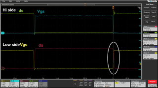
Question 1: Vgs turns hi already, but the Vds still kept hi, too. It makes me have poor efficiency and superheat. If TI experts can help me out with this, I will appreciate it.
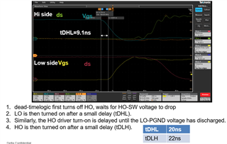
Question 2: I noticed the tDHL in spec needs 20ns at least. However, I overlap the Hi side and low side gs signal and the measured value is 9.1ns. I have no idea if it is correct. (waveform2) The phenomenon doesn't show up on the hi side mosfet turning on. (waveform3)
Thanks a lot ~
test condition:
Vin=24V
Vot=54V @ 3A
fsw=200kHz
Sway
waveform1:

waveform2:
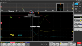
waveform3:

sch1: