This thread has been locked.

If you have a related question, please click the "Ask a related question" button in the top right corner. The newly created question will be automatically linked to this question.

CSD18502KCS: The Safe Operating Area (SOA)

Part Number: CSD18502KCS

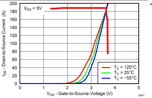
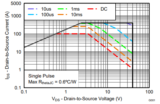
I try to understand the thermal instability limitation in the SOA, and it means that the MOSFET should operate at the negative temperature coefficient. However, according to the Transfer Characteristics of the datasheet, the area of negative temperature coefficient is over a certain value (IDS<180A), in other word, the larger IDS, the more stable. as a result, the safe operation area should be above the thermal instability limitation curve instead of below. I would like to know if there is a problem in my understanding. By the way, I want to know how this curve (thermal instability limitation) is measured.

  • Hello Steve,

    Thanks for the inquiry. For the SOA graph in the datasheet, the VDS/IDS operating point must always be below the line for a specific pulse width. Operating above the curve may cause permanent damage to the FET. The transfer characteristics in Figure 3 of the datasheet show the relationship between VGS and IDS. At values of VGS below ZTC (zero temperature coefficient), the drain-source current increases as temperature increases which may lead to thermal runaway. At values of VGS above ZTC, the drain-source current decreases with increasing temperature. Please see the app note at the link below. This includes links to all of TI's web based FET technical information. In it you will find a blog series on Understanding MOSFET datasheets including one on Safe Operating Area. Please let me know if you have any additional questions.

    https://www.ti.com/lit/an/slvafg3b/slvafg3b.pdf

    Best Regards,

    John Wallace

    TI FET Applications

  • Hi John,

    Thanks for your sharing. I have seen the series video about SOA, but I still have questions. As the saying that " At values of VGS below ZTC (zero temperature coefficient), the drain-source current increases as temperature increases which may lead to thermal runaway", so, the MOSFET should operate in the area that VGS above ZTC, and the corresponding drain-source current IDS should be over ZTC (over 180A). However, actually, the SOA shows that the IDS can not exceed 100A for DC.

  • Hi Steve,

    I consulted with a colleague who authored the Understanding MOSFET datasheets blog series.

    Basically, to avoid thermal runway completely you need to be operating the CSD18502KCS at VGS > 3.6V for VDS = 5V as shown in the transfer characteristics. When VGS is below the voltage corresponding to the ZTC point, the FET must be operated within the confines (below the line for a given pulse width) of the SOA graph. Therefore, at VDS =5V (from transfer curve), you would need to regulate the VGS to make sure IDS does not exceed the limit for a given pulse width in the SOA graph. SOA is an indicator of where thermal runaway can occur below that ZTC (VGS = 3.6V & VDS = 5V) point. It is a bit confusing but I think anytime you're operating the FET below ZTC, you need to make sure not to exceed the SOA limit. In fact, the FET should always operate below the SOA line for a given pulse width.

    Thanks,

    John

  • Many thanks for your answer.