This thread has been locked.

If you have a related question, please click the "Ask a related question" button in the top right corner. The newly created question will be automatically linked to this question.

TPS43061: Ultra-low ESR output capacitance with loop compensation triggers OverCurrent protection.

Part Number: TPS43061
Other Parts Discussed in Thread: CSD87350Q5D,

I'm designing a 12V21.8A input 20V12.5A output 96% efficiency boost power supply, using the MOS for the CSD87350Q5D power block.

The design switching frequency is around 820kHz (actual 790kHz), the current limit is 2mR (35.6A at D=40%), the detailed calculation parameters are located at the end of the article.

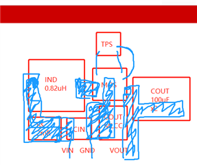
PCB layout ↓, all high current traces use 1x1mm copper strips to expand the current carrying.

The output capacitor is:

    2xGCM32EC71E226KE36L: 22uF ±10% 25V X7S (20V:-47%/11.6uF 900k:3mR Tc20C-0.8MHz:5A)
    1xTMK325B7226KM-PR:      22uF ±10% 25V X7R (20V:-82.9%/3.7uF 950k:3mR Tc23C-1MHz:4.4A)
    2x100uF 35mR Polarized Solid-State Capacitors For High Current Outputs
    1x22uF Unknown model of MLCC, he was able to attenuate ripple spikes in the test
    Total capacity 232uF, ESR 0.9mR, ripple current 14A

Calculated and practically used loop compensation parameters

    R_COMP=27.17k(30K)

    C_COMP=9.10n(10n)

    C_HF=30.24p(33p)

    These values passed the Webench power check and simulation.


However, the actual testing of this loop compensation parameter resulted in overcurrent protection.

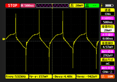
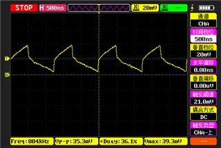
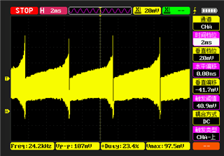
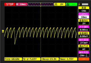
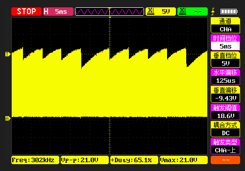
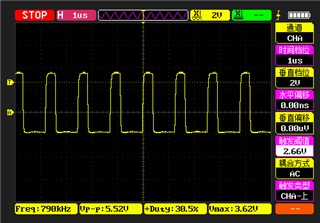
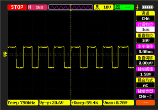
A 107mV peak appeared on the 2mR current detecting resistor (Fig. 1 below),

a recharge appeared on the SS capacitor (Fig. 2 below),

and the SW long time waveform (Fig. 3 below)

The HS control waveform, LS control waveform, and SW waveform,

are all normal except that the overcurrent protection is triggered,

but the duty cycle changes due to undervoltage caused by the current protection.

If I change the COMP values to:

    R_COMP=30K

    C_HF=10n

    C_COMP=33p

    By swapping C_HF and C_COMP, the power supply can output 20V10A stably.

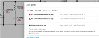
    However, Webench warns that this compensation value fails the check, suggesting that the phase margin is too low.

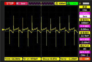
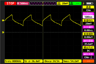
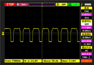
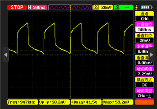
This is another test board pairing the C_COMP and C_HF current detection waveforms.

The switching frequency is 940k,

and the above problem also occurs when using the loop compensation parameters under theoretical calculations.

There is only a 58mV peak on the 2mR current detecting resistor (Figure 1)

I would like to inquire what causes this? And what to do to solve it.

    Why is there a peak current of about 50A at 100mV detected current when using COMP component parameters near the theoretically calculated values?

    As well as the fact that I am using a set of values that cannot be stabilized theoretically, yet I can maintain a stable 10A output?

Previously I also designed a test board for the TPS43061.

    It had used a CKG57NX7R1H476M500JJ double layer capacitor,

    two capacitors in parallel to get a low ESR output capacitor bank of 66uF 5mR or so, and an additional 330uF solid state capacitor to provide output current.

    The output can be stabilized without triggering the overcurrent protection using the calculated COMP compensation parameters.

C_OUT_LIST = [
    [11.6 * uF, 3 * mR],
    [11.6 * uF, 3 * mR],
    [3.3 * uF, 3 * mR],
    [5 * uF, 20 * mR],
    [100 * uF, 35 * mR],
    [100 * uF, 35 * mR],
]
        
===== DESIGN =====
V IN = 12.00V [11.80V~12.30V]     
I IN = 21.72A
POUT = 20V 12A
EMAX = 96.5%(-8.84W)
===== BOOST =====
Duty = 40% [38%~41%]
SW   = 823kHz MAX:2357kHz
RT   = 69.82kΩ
===== IND =====
L  = 0.80uH(0.82)
I  = 21.21A rms:21.31A peak:24.88A
RS = 2.00mΩ(<2.11mR) 2.59W        
CURRENT LIMIT = 35.65A(>33.75A)   
IND TD = 1.903W
===== MOS =====
I gd   = 23.39mA
P COND = HS:1.339W LS:0.392W      
P LOSS = SW:0.376W DT:2.238W      
TDP = 4.344W
===== CAP =====
V IN RIPPLE    = 37mV(60) 0.3%    
C IN           = 30uF(7.39)       
V OUT RIPPLE   = 26mV(200) 0.1%   
C OUT          = 232uF(31.13)     
C OUT ESR      = 0.90mΩ (6xCap)   
C OUT I RIPPLE = 10.60 A
===== CONFIG =====
R FB HS = 226.50kΩ
R FB LS = 14.70kΩ
C BOOT MIN = 0.034uF
C SS   MIN = 0.100uF
R UVLO HS = 47.00kΩ
R UVLO LS = 5.42kΩ
UVLO DIS:10.79V EN:11.61V
===== COMP =====
R COMP = 27.17kΩ
C COMP = 9.10nF
C HF   = 30.24pF
===== Freq =====
Adc    = 17.70V/V
f_Pmod = 0.43kHz
f_Zmod = 0.76MHz
f_RHPZ = 110.70kHz
f_co1  = 27.68kHz
f_co2  = 164.70kHz
f_co   = 27.68kHz

  • Hi, 

    不好意思, 您这颗芯片不是中国team在看,所以麻烦您这边坐下英文描述,谢谢。

    Regards

    Tao

  • 好的,我翻一下

  • Hi,

    Thread assigned to my colleague, please waiting his response.

    Regards

    Tao

  • Hi zbqin,

    Thanks for using the e2e forum.
    Please allow me some time to forward this thread to a colleague who can support you speaking Chinese as well.
    We will get back to you within the next two days.

    Thanks and best regards,
    Niklas

  • Hi zbqin,

    As the thread has been translated, I can give my inputs as well:

    For calculating the compensation, have you only used the webench calculator?
    We have a quickstart calculation tool for TPS43061 as well.
    https://www.ti.com/tool/download/SLVC471

    If this is a stability issue, you may also check the design stability by using a Bode Analyzer, or make a load transient measurement if no bode analysis is possible.

    Would you be willing to share a schematic of your design as well?
    This would help me in finding the source of this issue.

    Best regards,
    Niklas

  • The schematic is referenced from Datasheet 9.2 Typical Applications.

    I don't have an instrument for power supply testing and the oscilloscope is too slow to capture the load response.

    I can't confirm if it's a stability issue as it appears to simply trigger the overcurrent protection, and then I found a temporary solution on a board that had a manual soldering error (swapping C_HF and C_COMP)

    The results calculated using the Excel file are consistent with the results obtained from the datasheet's formulas.

    Vin min 11.8 V
    Vin nom 12 V
    Vin max 12.3 V
    Vout 20 V
    Iout 12.5 A
    RSH 226500 Ω
    RSL 14700 Ω
    RCOMP 25500 Ω
    CCOMP 2.2E-9 F
    CHF 22.0E-12 F
    fsw 800000 Hz
    L 820.0E-9 H
    DCR 0.00167 Ω
    Rdson 0.0042 Ω
    Co 223.0E-6 F
    Co ESR 0.001 Ω
    Risense 0.002 Ω

    V IN = 12.00V [11.80V~12.30V]
    I IN = 21.72A
    POUT = 20V 12A

    SW = 823kHz MAX:2357kHz
    L = 0.80uH(0.82)
    I = 21.21A rms:21.31A peak:24.88A
    RS = 2.00mΩ(<2.11mR) 2.59W
    C OUT = 232uF(31.13)
    C OUT ESR = 0.90mΩ (6xCap)
    R FB HS = 226.50kΩ
    R FB LS = 14.70kΩ
    R UVLO HS = 47.00kΩ
    R UVLO LS = 5.42kΩ
    R COMP = 27.17kΩ
    C COMP = 2.12nF
    C HF = 21.17pF

  • Hi zbqin,

    Thanks for the additional information.
    I will discuss this issue internally and will get back to you with additional suggestions tomorrow.

    Best regards,
    Niklas

  • I did more testing and if I change the C_HF capacitance value to 1nF and RC_COMP to 30K and 10nF respectively, the output can stabilize for more than 30 minutes and maintain 96% efficiency with current sensing of 58.2mV. but the simulation will warn of too low phase margins.

    I would also like to ask about Webench calculations for temperature, a few days ago I was going to reconfigure the simulation current size, if I continue to set the 15A output Webench pops up that the temperature is too high not to allow to keep that configuration, I have to lower it to 12A and set the ambient temperature to 0 degrees in order to save it and the junction temperature in the picture above appears to be too high and does not allow me to run the simulation calculations. But today when I changed the output current again from 12A to 15A, Webench did not stop me and the high junction temperature warning disappeared after saving the configuration.

  • Hi zbqin,

    Thanks for the update.
    Sadly I have very little experience on the webench simulation, therefore I cannot tell where the original warning comes from and why it suddenly disappeared at even higher loads. As the power ratings mainly affect the power stage components (FETs, inductor & output caps), please make sure these components have sufficient ratings.
    Looking once more at the first waveforms you sent, it looks like the signal is rising linear at first, but then takes an upwards slope. This could be a sign of the inductor falling into saturation. Can you please make sure that the inductor can supply the worst case current + additional ripple?

    Thanks and best regards,
    Niklas  

  • The inductor is an FXL1350-R82-M (DCR=1.67mR Isat=39A Irms=30A) which is capable of meeting the calculated inductor current.

    I have some other waveforms which are the result of an early evaluation of this power supply scheme using two CKG57NX7R1H476M500JJ output capacitors. The actual output capacitor values were 2*36.9u+330uF with ESR=5.5mR. but after I replaced the capacitors with ESR=0.9mR 23uF+200uF the inductor current became that.

    This capacitor was discarded due to high temperatures caused by a ripple current of only 2-3A.

    But the waveform is better than the current replacement ultra-low ESR capacitor except for some spikes.

  • Hi zbqin,

    Regarding the mentioned ceramic capacitors. When using ceramic caps rated for 25V for an application with 20V output voltage, you will have a derating of the actual capacitance value due to DC bias.
    This means if the cap has 23uF at 0V, it can loose more than 40% of its actual capacitance when operating at 20V DC voltage.
    An example of DC bias rating is normally given in the capacitor datasheet:

    If there is a large ripple at the output voltage with the same frequency as the switching frequency, it is often caused by too low ceramic capacitance.

    Best regards,
    Niklas

  • I understand the problem, so I choose almost always capacitors with low DC bias loss (-50%) and these are capacitor samples are expensive, some of the cheap capacitors lose 75% of their capacity at 20VDC bias.

    But if I use parallel capacitors to compensate for the capacity problem, it results in a very low ESR. The EIA-1210 capacitor with the largest actual capacity at DC bias that I could get samples of was the GCM32EC71E226KE36L (11.6uF), but he had an ESR of 3mR at the switching frequency, and if I wanted to get 70uF I would need 6 capacitors, and then the total ESR would go down to 0.5mR. and then I would run into the overcurrent protection problem mentioned in this article. At the moment I can get around the problem of triggering the overcurrent protection by using a larger C_HF, but I'd like to know why as I don't have the instrumentation to test the power supply to see if the loop response curve passes.


    That inductor current waveform I tested at low loads and it didn't change at 5.6A loads and 10A loads except for a different max voltage. The only difference from the previous evaluation board is that the output capacitor is different, but the connection to the output capacitor should be cut off by the high side MOS when the inductor is charging, what is causing the inductor current waveform to lose the triangular wave appearance?

  • Hi zbqin,

    The connection to the output is never fully cut off in a boost topology. This is also the case for a synchronous design using two FETs, as the current can still flow through the body diode of the high side FET when the gate is turned off, and you will also still have reverse recovery effects.

    Best regards,
    Niklas