This thread has been locked.

If you have a related question, please click the "Ask a related question" button in the top right corner. The newly created question will be automatically linked to this question.

TPS552882-Q1: TPS552882-Q1的buck-boost mode

Part Number: TPS552882-Q1
Other Parts Discussed in Thread: TPS552882, TPS55288

hello,

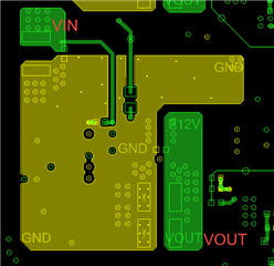
TPS552882-Q1 Why is it always buck first and then boost in buck-Boost mode?

In theory, when VIN<VOUT, should be boost first, then buck; When VIN>VOUT, it should be buck first and then boost.

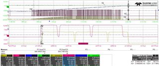
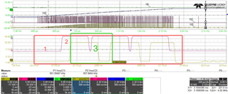
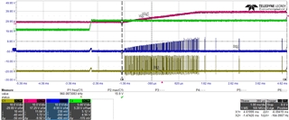
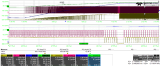
Waveform as follows:

The waveform at 9.8V
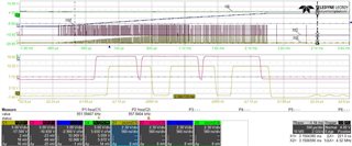
The waveform at 13V

  • Hi Seven,

    When exiting skip mode and starts switching, the first cycle would be Buck high-side on and Boost low-side on. It is not decided by Buck or Boost mode.

    BRs,

    Bryce

  • Sorry, I meant:

    First of all, my output is 12V. Since my input voltage is close to the output voltage,When the TPS552882 works in buck-boost mode, for example, when the input is 11.5V, it is buck first, then boost in this mode, right? When the input is 12.5V, the mode is once again boost, then buck, right?

    However, I found that in both cases, it was first buck, then boost. Therefore, I would like to ask how the TPS552882 works under buck-boost model.

  • Hi Seven,

    How do yo define which mode is first? I think the sequence is not meaningful at PFM mode. As I mentioned, when exiting the skip mode, the first cycle is Buck high-side on and Boost low-side on, then Buck high-side and Boost high-side on.

    BRs,

    Bryce

  • Hi Bryce,

    Thank you very much for your reply. I would like to ask again why the PFM model is such a process as you answered?

  • Hi Seven,

    In buck-boost mode, the first cycle is used to magnetize the inductor to increase the inductor current, so Boost Low-side FET is on first.

    BRs,

    Bryce

  • Hi Bryce,

    Thank you very much.As shown in the figure, what number does this first cycle correspond to in the graph? How can I explain the three serial numbers of my marked?

  • Hi Seven,

    The '1' phase is still the skip phase which is non switching phase. The '2' phase is the first cycle I meant, Buck high-side on and Boost low-side on. The '3' phase is Buck high-side on and Boost high-side on. You can probe the inductor current waveform for better understanding.

    BRs,

    Bryce

  • Hi Bryce,

    So four swithchings are off in the '1' phase,right?

  • Hi seven,

    Yes, no switching in phase 1.

  • Hi Bryce,

    The question I asked you about TPS552882 is because there are two cases of TPS552882QRPMRQ1 burning problem. The investigation found that the high-side and low-side MOSFET of the chip were burned, and the two external MOS were also burned.

    The schematic diagram is as follows:

    Can you give me some clues about this failure?Or what will cause MOSFETs to burn?

    Thank you for your help very much.

  • Hi Seven,

    1. May I know what is the application and product type here?

    2. What is the input voltage range, output voltage range and max output current?

    3. Do you have the part number of the output caps(C9305-C9308)?

    4. Can you also share with your layout?

    BRs,

    Bryce

  • Hi Bryce,

    1.This is used to power camara;

    2.the input voltage range is 9V to 16V ,output voltage is 12V and max output current is 5A,another the ILIM=8.2A;

    3.the part number of the output caps(C9305-C9308) is GCM32ER71E106KA57L form MURATA;

    4.layout

  • Hi Seven,

    Thanks for the feedback, may I know what is the customer and the project?

    And which test do you found the device damaged? In startup test or steady state test? Do you have any waveforms at the time the device failed?

    Which vendor of MOSFET is populated at the damaged board?

    The layout looks ok for me, but I think the switching frequency is too high for this power level, the thermal would be a large concern. And the total effective output capacitance is only 41uF, which would also cause poor transient response.

    BRs,

    Bryce

  • Hi Bryce,

    1.This IC is used by our NIO in the automobile AD domain control;

    2.This is the after-sales fault part. when the owner starts the fault is found, and then read the output voltage through the log is 0V, and the EN is high; After the disassembly locates this chip and the external MOS burned;

    3.This MOS is DMT47M2SFVWQ-7 in DIODES.

    4.How much output capacitance do you recommend to increase the transient response?

    5.A similar thing happened to our IC last year, when the FPWM mode was used, and then the PFM mode was changed to reduce the probability of failure. However, now such measures have not prevented such problems from happening, so can you find a possible reason for such failures from inside the IC? 

  • Hi Seven,

    Thanks for the details.

    1. May I know how many cases were found failed in this project?

    2. Is there any case only Buck side FETs damaged and TPS55288 is ok, or the opposite condition?

    3. Could the board output 12Vout/5A from 16Vin? From my point of view, the MOSFET is a risk to output such high power level. From the calculation, with 10mohm Rdson, the power loss of Buck LSFET can be up to 2W which could result in 100C temp rise, so I am wondering if the Buck side FET is damaged first, and then TPS55288 got damaged.

    4. The output capacitance is decided by the undershoot/overshoot requirement during the load/line transient and voltage ripple. Typically, the transient response needs more capacitance.

    5. Yes, I saw you set the mode to PFM, so I don't think it is related to that.

    BRs,

    Bryce

  • Hi Bryce,

    1. At present, two cases have occurred in my project.

    2. You can confirm that there are two faulty components. The TPS552882 internal BOOST side of the high and low side MOS are bad, the external BUCK side of the high side MOS is bad, or high side and low side MOS are bad.

    3.To correct a problem, although we designed this output current as 5A, the actual maximum current is only about 1A, so I think there should be no problem of too much power and poor transient response.

  • Hi Seven,

    Thanks for feedback.

    Do you have any idea about in what condition the device can get damaged? It would be much better with the operating condition to replicate the failure.

    BRs,

    Bryce

  • Hi Bryce,

    Unfortunately, I didn't replicate it, so I wanted to ask you for some clues to help mereplicate it.

    I suspect that because of the logic error of the IC, the low MOS inside the IC was opened at an inappropriate time, resulting in VIN being overloaded to the ground for a long time. This phenomenon is basically similar to what happened before, and the cause of failure is also basically similar, so I would like your company to give clues from inside the IC.

  • Also, we have another case today, and the phenomenon is consistent.

  • Hi Seven,

    I suspect that because of the logic error of the IC, the low MOS inside the IC was opened at an inappropriate time, resulting in VIN being overloaded to the ground for a long time.

    May I know which low side do you mean? Buck low-side or Boost low-side? Do you have any waveforms and operation conditions with this?

    This phenomenon is basically similar to what happened before, and the cause of failure is also basically similar, so I would like your company to give clues from inside the IC.

    The phenomenon you mentioned is different from this because this device only works in PFM.

    Also, we have another case today, and the phenomenon is consistent.

    Is the same project with this? And the same schematic and layout?

    BRs,

    Bryce

  • Hi Bryce,

    1.the low side of BOOST,There is no recurrence, so there is no associated waveform.

    2.Changing PFM is only a measure to reduce the failure rate at that time, and it does not mean that PFM can be completely covered.

    3.All the same.

  • Hi Seven,

    Thanks for feedback, since PFM is enabled, the zero-crossing function is always on during all the operation period, and there will be no negative current, so I don't think this can be the same reason as before.

    For this case, can you help do some test and probe some waveforms of the startup and load transient?

    BRs,

    Bryce

  • Hi Brycle,

    I would be happy to provide some test waveforms.

    Light load:

    heavy load:

    From these waveforms, it seems to be fine, but unfortunately, this failure occurred. Do you have any good ideas to help me reproduce the faulty waveform?

    And from our design point of view, behind the TPS552882, we have a POC switch, which has a 300mA current limit, so it can not be the overload caused by the short circuit of the rear load, only TPS552882 itself has a short circuit, resulting in such a serious burn.

  • Hi Seven,

    Thanks for the waveforms, I agree with you that the waveforms look good. And if you probe the inductor current, you will not see negative current at light load or heavy load. So I am not quite sure about the clues that can reproduce the failure, do you have any idea if the failure happens at some specific temperature?

    BRs,

    Bryce

  • HI Bryce,

    However, at present, the IC did burn down. From the log of our latest case of failure, it seems that the failure occurred when the power was already stable, and the temperature sensor near us detected a temperature of more than 85°C at the time of failure, which should be the high temperature brought by the burning. In addition, we use liquid cooling to dissipate heat, so the temperature inside our board is generally not more than 75°C.

  • Hi Seven,

    Do you have the idea which device is damaged first? Buck FET or the chip?

    If the failure is detected during the steady state, can you make the board running and use single mode to probe the Vout, iL, SW1 and SW2 waveforms at the time of the failure?

    BRs,

    Bryce