This thread has been locked.

If you have a related question, please click the "Ask a related question" button in the top right corner. The newly created question will be automatically linked to this question.

TPS55288: parasitic current draw on custom design

Part Number: TPS55288


Hello,

I have a question about the TPS55288 IC.

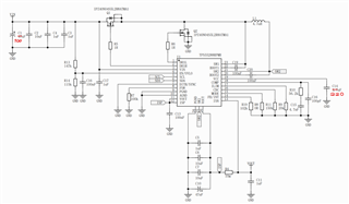
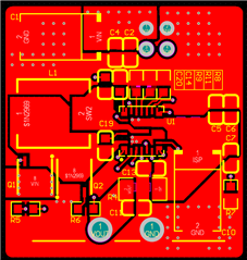
I have designed and made a schematic and PCB with the exact same components as the TPS55288EVM-045 Evaluation Board, and placed them on a much smaller PCB (about 25mm x 30mm) and I have noticed some unexpected behaviour:

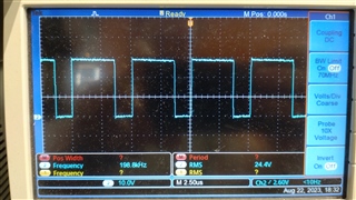
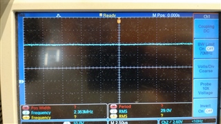
When setting the output to 20 Volts via I2C and having no load on the output, the evaluation board draws 6mA of current and no components excerpt any noticeable amount of heat (recorded with FLIR thermal camera). When using the same component setup and the sending same I2C command to the custom made PCB, the current draw starts out at ~120mA and ramps down to ~16mA (again, no load), and the inductor on the board starts rapidly heating up to around 70 degrees C.

I have verified all resistance paths and connections to be the same as the Eval. board, tried different capacitor and inductor combinations, varied the switching frequency, nothing removes this parasitic draw.

Any help would be appreciated, thank you!

  • Hi Dominykas,

    Thanks for reaching out.

    1. May I know what is the application and product type here?

    2. What is the input voltage range, output voltage range and max output current?

    3. Can you also reply with the schematic and layout of the customer board?

    4. Do you have any waveforms including SW1, SW2, Vout, iL and Vin?

    BRs,

    Bryce

  • Thank you for your response,

    1. PD power supply

    2. Input - 24-28V, Output - 20V 3A

    3. 

    4. SW1: 

    SW2: 

    Vout: 

    Vin: 

  • Hi Dominykas,

    Here are my comments.

    1. About the schematic:

    (1) What is the part number of the inductor and output capacitors C6,C7,C10?

    (2) If FB/INT is not used, you can leave it floating.

    (3) Do you used 220uF as the VCC cap?

    2. The layout is very poor from my side, especially the output cap position is very far away Vout and GND pins. You can refer to this layout guideline for more details. www.ti.com/lit/an/slvaer0b/slvaer0b.pdf

    3. I don't see anything abnormal from the waveform, are these waveforms captured from TI EVM or the small board? Can you probe the waveforms of the inductor current and SW1, SW2 at the startup period when you find the current draw starts out at ~120mA and ramps down to ~16mA (again, no load)?

    BRs,

    Bryce

  • Hi Dominykas,

    We have not seen an update from you for two weeks, so I assume the questions are answered.

    I close this thread now. If there is still something open, please reply and the thread will get opened again.

    If you have any other question or of the thread has been locked, please open a new one.

    Best regards,

    Bryce