This thread has been locked.

If you have a related question, please click the "Ask a related question" button in the top right corner. The newly created question will be automatically linked to this question.

BQ40Z50: Cell balancing internal bypass

Expert 3511 points
Part Number: BQ40Z50

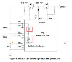
Section 8.3.5.5 mentions that "The device supports cell balancing by bypassing the current of each cell during charging or at rest. If the device's
internal bypass is used, up to 10 mA can be bypassed and multiple cells can be bypassed at the same time.
Higher cell balance current can be achieved by" 

Is it more accurate to say 10mA at a minimum instead of "up to 10mA"

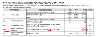
Section 7.10 "Electrical Characteristics: VC1, VC2, VC3, VC4, BAT, PACK"  specifies that the internal balance FETs are 200ohm max, over a range of 2V to 4V.

So the balance current can really be 2V/200R (min of 10mA) but if we are nearing full charge, then 4V/200R = 20mA.

We probably care more about balance around the 3.65V area, so 18.25mA balance current.

Also, the FET res of 200ohm is MAX value over temp and processing, so the typical value of balance current should be much higher than 10mA.

Please let me know your feedback! 


Thanks

  • Hello JDJ,

    The up to 10mA means that a maximum of 10 mA can flow thought the internal bypassed FET. See below for a similar internal FET demonstration.


    The internal FET balance resistance has a maximum Rds(ON) of 200 ohms. With the known internal maximum cell balancing current Icb_max (10mA), to achieve Icb_max it is required a cell voltage of 2V. If the user has a 4V cell, ideally the maximum internal cell balancing current will be 20 mA, but the gauge will not allow this as Icb_max is 10mA.

    If customer wants a bigger balancing current, external circuitry configuration will need to be used for bigger balancing current where most of the current will be dissipated in the external balancing FET and only <10mA will be dissipated in the internal balancing FET (assuming the external circuit design is correct). For more details on how to perform external Cell Balancing, please reference to the Fast Cell Balancing Using External MOSFET app note.

    For any other questions on how the internal cell balancing algorithm runs, please reference to the Cell Balancing Using the bq20zxx. Notice it is a different device but same balancing principle.

    Regards,
    Jose Couso

  • Hi, Jose Couso,

    I have a question about the internal cell balance resistance. As defined in the datasheet of BQ40z50, the internal cell balance resistance for internal FET switch at 2 V < VDS < 4V is 200ohm max. Does the VDS means the cell voltage? If cell balancing current Icb is 10mA and the internal cell balance resistance is 200ohm, the Drain to Source voltage of the internal switch is 2V. However, the Rvc in external RC filter is 100ohm and the drop voltage in the two Rvc resistence is 2V (10mA*100ohm*2=2V). So the cell voltage is 4V. Will cell balance work at 4V cell voltage?

    Besides, if multiple cells are bypassed at the same time, how to calculate the cell balancing current?

    Looking forward to your reply!

  • Hi Chong Shen,

    Please refer to Section 2.1 Internal Cell-Balancing Circuit Design from this App Note

    Note it is a different device but same principle.

    Regards,
    Jose Couso