This thread has been locked.

If you have a related question, please click the "Ask a related question" button in the top right corner. The newly created question will be automatically linked to this question.

LM5122: LM5122 boosting function failure issue

Part Number: LM5122

Hi Sir,

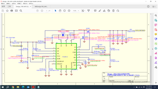
We had already referred to the reference design(WBDesign198_LM5122MH_reference design, designed from TI side) to finish our schematic(Design_198 LM5122MH_NOPB) but the LM5122 boosting function failed fully.

The target specification is listed below.

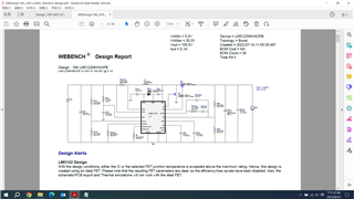
Design : 198 LM5122MH/NOPB
LM5122MH/NOPB 5V-30V to 100.00V @ 0.1A

VinMin = 5.0V
VinMax = 30.0V
Vout = 100.0V
Iout = 0.1A

Device = LM5122MH/NOPB
Topology = Boost
Created = 2022-07-14 11:05:35.467
BOM Cost = NA
BOM Count = 26
Total Pd =

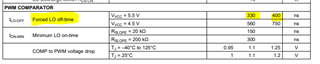
TI's on-line FAE had ever pointed out the boosting function failure should be caused by the Q2 mosfet which is with incorrect pin design in my schematic, the drain pin and source pin shall be swapped to have a correct design.

I did follow this comment and replace with a new mosfet(with the totally same part) and get the two pins swapped but the boosting failure is still the same. That is the Vout voltage(DC 10V) is almost same as Vin(DC 10V) under no load condition so far.

Can you please kindly advise me how to fix this boosting failure issue?

Much appreciated in advance!

Best Regards,

Bob Chen 2023/08/23

  • Hi Bob,

    Thanks for using the e2e forum.
    At a Rt resistor of 169kOhm, the device should run close to minimum fsw with 55kHz.
    At this fsw, there should be no violations of minimum on-time of the device, even in worst case condition.
    However, this also means the inductance needs to be much higher to support the output power of 100V/0.1A.

    Our power stage designer tool recommends an inductance of 4.5mH for this application, which would be much higher than the 470uH inductor used.

    Two more questions from my side:
    - The schematic shown is before changing the drain and source of the Q2 FET, correct? It is still wrong in the schematic
    - Can you send a waveform of the switch node behavior? Is the device not switching at all, or is the device not able to reach the 100V output?

    Thanks and best regards,
    Niklas

  • Hi Niklas,

    Thanks for your comments.

    For your two questions, my replies are listed below.

    [Question 1] Yes, the attached schematic is the original one before actual on-board modification. For now, I have got the drain and source pins swapped on  Q2 but the boost function still failed. The Vout is almost same as Vin when Vin is 10Vdc under no load condition.

    [Question 2] I fail to send you the waveform of the switching node since the device is with no switching at all.  

    Since the existing inductor is with quite big size(ring type with over 20mm diameter) to my board size, we fail to accept much higher inductance with bigger size.

    After internal discussions, we can greatly downgrade the requested specifications in order to keep using this existing inductor(470uH) and most existed parts if possible!

    The updated specifications is listed below.

    Vin : DC9V ~ DC15V(typical = DC12V)

    Vout : DC100V @0.1A(100mA) rating

    Please kindly advise us if this target above can be reachable??

    Thank you so much.

    Best Regards,

    Bob Chen 2023/08/25 

  • Hello Bob,

    Is it mandatory that you are operating the boost controller at such a low switching frequency?

    Thanks and regards

    Harry

  • Hello Harry,

    Based on keeping the same(original) inductor, we can accept higher switching frequency!

    Please kindly advise us the whole system solution soon.

    Thank you so much.

    Best Regards,

    Bob Chen 2023/08/30

  • Hi Bob,

    Thanks for your feedback.

    Assuming the 470uH inductor is fixed, a suitable switching frequency would be ~500kHz.
    Now looking at the worst case situation with min Vin (5V) and max load, there would be a duty cycle of 95% with LO side off-time of ~100ns.
    This would contradict with the minimum off-time requirements of the IC, given by the datasheet:

    They should be able to increase the switching frequency to 150kHz and still align with the min off-time requirements. This should already improve the behavior. For higher switching frequencies, they would need to increase the min. Vin spec to achieve higher worst-case duty cycle.

    Now it would be for the customer to decide with trade-offs fit best for them:

    - Increase switching frequency ( this would require to increase spec for min. Vin to reduce duty cycle and align with min off-time requirements)
    - increase inductor
    - change to a flyback topology

    Best regards,
    Niklas