A related question is a question created from another question. When the related question is created, it will be automatically linked to the original question.
If you have a related question, please click the "Ask a related question" button in the top right corner. The newly created question will be automatically linked to this question.
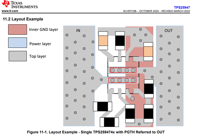
Yes vias are recommended. The vias under the device also help to minimize the voltage gradient across the IN and OUT pads and distribute current uniformly through the device, which is essential to achieve the best on-resistance and current sense accuracy.