This thread has been locked.

If you have a related question, please click the "Ask a related question" button in the top right corner. The newly created question will be automatically linked to this question.

TPS1HC100-Q1: TVS diode for clamping

Part Number: TPS1HC100-Q1
Other Parts Discussed in Thread: TPS1HC30-Q1, TPS272C45

Hello,

I am using a high-side driver (TPS1HC100-Q1) to drive an inductive load.

The single pulse turn-off energy for this high side driver is 35mJ.

But, energy stored in the inductor is much higher than this.

So, while turning off the high-side driver there is high probability that the driver would get damaged.

I am planning to use an external TVS diode connected across the drain and source of the high-side switch with lower clamp voltage compared to the high-side switch as a work around.

Not sure if inductance of the leads and tracks would allow the current to switch from the high-side driver to the TVS diode when the high side driver turns off.

Request your comments on this.

  • Hi Salil,

    We have used external Vds clamps to "undercut" the internal clamp in some applications. The trace/pad inductance is minimal.

    Since the external load is pulling the output voltage low, the external Vds clamp will trigger first. I have not personally seen the edge case event you are describing, but in such an event if the Vds voltage flies large enough for the internal Vds to trigger, this predicates that the voltage difference would be large enough for the external Vds to clamp or start clamping. Since the internal path is more resistive than the external path, current will shunt through the external path and the voltage will recover to the external clamp level reducing any time duration where it would flow through the internal path.

    Thanks,

    Shreyas

  • Hi Shreyas,

    Thank you for your reply.

    I have couple of questions more:

    1) Could you please provide the single pulse energy capability of TPS1HC30-Q1 ?

    2) What would happen to the IC when the coil tries to dissipate energy in the HS switch which is more than its capability ?

    Does the IC protect itself with a thermal shutdown? 

    Kind Regards,

    Salil

  • Hi Salil,

    1. The single pulse energy for TPS1HC30-Q1 is 65mJ and this was tested at 13.5V, Ta=125C and with a 1.5mH load.

    2. Inductive dissipation occurs when the device is OFF. In normal circumstances when the device is ON, the device protects itself by turning off and reducing the energy dissipated such as thermal shutdown. Since this cannot occur during inductive turn off, large energy stresses on the device can lead to degradation of the FET and a reduction of lifetime. It can also lead to device damage. Therefore, if the load is expected to be heavily inductive in nature, we recommend the use of external clamping.

    Thanks,

    Shreyas

  • Hi Shreyas,

    Would you please provide examples of how an external clamping circuit would look like ?

    Are ESD suppressors good alternatives to TVS diodes for external clamping?

    kind regards,

    salil

  • Hi Salil,

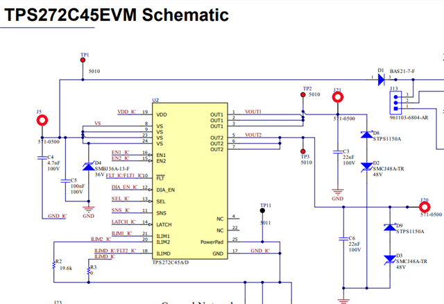
    1. We have no dedicated recommendation. External clamping can be achieved by using a TVS from output to GND as shown in this example of an industrial device:

    A TVS diode in series with a Schottky is used to avoid conduction during normal operation.

    Another option is to use a TVS diode from the VS pin to the VOUT pin. This is essentially to build an external drain to source clamp just like the clamp within the device. 

    In both cases, the recommendation is to select a clamp that triggers before the internal clamp. Please check the device datasheet to view the minimum Vds clamp level.

    2. Usually ESD diodes do not have the power capability required to demagnetize an inductive load. We recommend using external TVS clamps.

    Thanks,

    Shreyas

  • Hi Shreyas,

    Thank you for your reply.

    For my application, Vs to Vout clamp would be feasible as the coil being driven is not connected to ground.

    How much difference do you recommend between the minimum Vclamp of the IC and the clamp voltage of the external TVS diode?

    Also, do I have to take care of any special layout considerations for the external TVS diode?

    kind regards,

    Salil

  • Hi Salil,

    No special layout considerations are needed but we do expect this TVS device to see all the inductive energy. Therefore, it would be beneficial to place the TVS close to the device and to make sure there is sufficient copper on the board to act as a heatsink.

    The minimum Vds clamp voltage for TPS1HC30-Q1 is 33V across temperature. We have seen TVS diodes available in specific voltage offerings. I would suggest 24V TVS diodes. This should have a breakdown voltage around 28V or so which is further away from 33V. If you are able to find a higher voltage TVS diode, this is also acceptable but do note that often the breakdown voltage is a little higher than the clamp voltage and to effectively circumvent the internal diode, the TVS must trigger first.

    Thanks,

    Shreyas

  • Hi Shreyas,

    Thank you for your answers. I have a clearer idea now.

    Couple of more questions:

    1) The datasheet for TPS272C45 on page 3 advices to use 'C' version of the device because it 'enables usage of external TVS diode for high inductive loading'. 

    Is there any similar issues with TPS1HC30-Q1 ?

    2) For the external clamp across Vs and Vout, is a schottky diode advised in series with the TVS ?

    Kind Regards,

    Salil

  • Also, I did a spice simulation with TPS1HC100-Q1 as no spice model is available for 30-Q1.

    It was seen that the Vout pin faces a negative voltage of around -6V to -7V max for around 2ms.

    The VBB pin is clamped at 16V from external supply.

    Please also advice if this negative voltage at Vout might be detrimental to the IC.

  • Hi Salil,

    1. Only our industrial portfolio has non Vds clamp versions. All our automotive device have an integrated clamp.

    2. For an external clamp across VS and Vout a Schottky can be used to block the reverse conduction path in the event reverse polarity is a concern. But this is not necessary since the FET turns on in the reverse condition to conduct as well. A Schottky can be place before the device and act as the upstream reverse protection for the device as a whole eliminating the need for a GND network.

    3. The output of the device is compatible to go as low as the Vds clamp allows. For example if the voltage is 12V and if the Vds clamp is 40V, during turn off, the output voltage is expected to reach -28V before the clamp kicks in. The device is built to handle these inductive negative spikes. 

    Thanks,

    Shreyas