This thread has been locked.

If you have a related question, please click the "Ask a related question" button in the top right corner. The newly created question will be automatically linked to this question.

UCC23511: Why almost all gate driver ICs have a relative large on-resistance for their MOSFETs of driving structure.

Part Number: UCC23511

I'm now designing a gate driver operating at high switching frequency for a relative large gate charge device. I noticed that the internal on-resistance of the driver leads to significant thermal effect. This thermal is supposed to be undertaken by external gate resistor, which is outside the IC and has more flexibility on thermal design. I feel confused why almost all gate driver ICs in the market have a relative large on-resistance (turn-on/turn-off), because in my understanding, the low voltage (<80V) MOSFET can be manufactured with tens of milliohms for RDS (on) easily. Could you please tell me which aspect determines this feature? I can only guess possible reasons as following:

1. Cost Consideration? The relative large RDS (on) MOSFET is much cheaper than lower one, and the internal RDS (on) does not cause significant thermal issues for most applications.

2. Area of die? The large RDS (on) can cause an unacceptable large area of the die or it is unnecessary to waste area on this feature given that gate driver application? 

3. Reliability? The large RDS (on) can bring better reliability on EMC or fault protection or other aspects?

4. Easy to use? In some cases, the external gate resistor is not needed, the relative large resistance can provide a basic gate resistance value for potential resonant damping. 

Thank you for answering this question! Could you please share any link talking about this issue if available? 

  • Hi Liyang, 

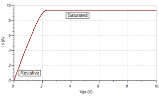
    The CMOS output stage has the I/V characteristic of a MOSFET. The output resistance is only valid when the output current is low and the voltage is pretty close to the rail. At the initial condition, when the gate driver output is starting to drive the gate, saturation current is the more important metric. You are correct that the die area and cost are higher for a larger, lower resistance output stage. For an isolated gate driver like UCC23511, another important factor is is that the TX and RX functions also must take up some room inside the device package. These are more easy to implement with a CMOS process. The 10s of mOhm MOSFET is just one big transistor.

    Our smaller drive strength drivers do often leave some efficiency on the table, and you can add a discrete output stage using external components that is more powerful than the integrated gate drivers. Externally, you can even use bipolar junction transistors, which will have a lower output resistance for the same output current vs. CMOS.

    There is a limit to how large you want to make the output stage transistors however. The whole point is to drive a parasitic Vgs capacitor. If your output stage itself has a significant self-capacitance, the overall turn-on time will be slower than for a more appropriately sized output stage bandwidth.

    Every switch will have its own optimal gate driver size, and it is important to test a few to get a better understanding of what size is best. Weaker driver are harder to damage, which is something customers also are very concerned about.

    I am currently working on an output stage comparison, and I hope to have a link with a more in-depth explanation in the near future.

    Best regards,

    Sean

  • Thank you Sean! That is very helpful and resolved my question!

    Best Regards,

    Liyang