This thread has been locked.

If you have a related question, please click the "Ask a related question" button in the top right corner. The newly created question will be automatically linked to this question.

TPS54531: Audible switching noise during on high load

Part Number: TPS54531

Hi,

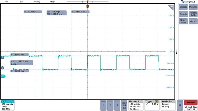
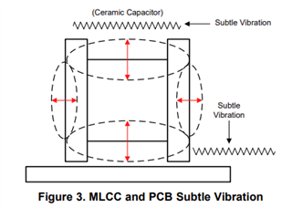
We are using the TPS54531DDA for generating a 5V with current requirement of 2.7A (at max load) from 12V to 19V input voltage. at high load condition, we are able to hear the switching noise from this regulator section. we are not able to hear this kind of noise during light load. Could you help me to sort out this issue?

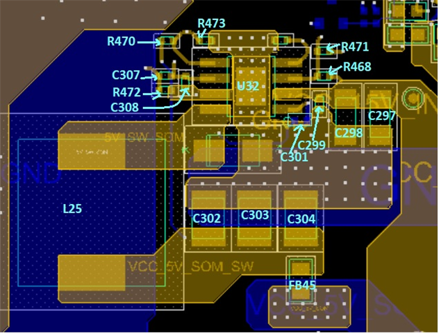
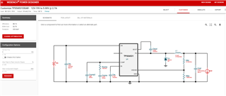
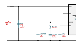
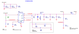
Please see the schematics of regulator design below.

Thanks,

Jab

  • Hello Jab,

    1. Could you please provide SW/Vin/Vout waveforms? I would firstly check whether the switching pulses are stable or not. If the SW pulses were unstable, and oscillation frequency within 20Hz~20kHz audible frequency range, you may hear audible nose. If you saw unstable SW waveform, please adjust Comp network (refer to Webench tool recommended circuit) to make sure SW stable.

    2. Could you please check where does the noise come from? From inductor or from MLCC output caps? You can re-solder the inductor, only connect one pin of inductor to board, using a wire to connect the other pin of inductor to board, if the noise could be removed, the noise should come from inductor. Sometimes using different L or Cout may improve audible noise. I saw cases that changing MLCC from big size to smaller-size could solve the MLCC audible noise issue.

    3. Could you please share layout file? I will review it.

  • Hi,

    Thanks for your reply,

    1.  Please see to the regulator's SW node waveform. It appears that the switching pulses are stable.
    2. We resoldered the inductor and connected with regulator side, cap side by suing the wire. It seems that the switching noise is being produced by the regulator or capacitor side, not the inductor side. We noticed decrease in the volume of switching noise after changing the resistor and capacitor values in the compensation network (C307 and R472 in the schematics above that are attached) to 30k and 3nf, respectively. Could you kindly explain why the switching noise volume decreased after modifying the compensating network? Can we eliminate the switching noise by changing value of parts used in the compensation network?
    3. Please the layout attached layout image below for reference.


    Please let me know if you required any other details.

    Thanks,

    Jab

  • Hello Jab,

    Thanks for your provided information. My comments are below.

    1. Is the waveform captured when you heard audible noise? You may capture Vout ripple waveform, check whether has 20Hz~20kHz low-frequency oscillation.

    2. From your description, the audible noise doesn't come from inductor, then it should come from output MLCC caps, not from IC. Because MLCC uses dielectrics with piezoelectric characteristic. Below figure shows when the AC voltage is applied to MLCC, the dielectrics will cause a subtle vibration by expanding and contracting, and the vibration travels to PCB surface. If the AC frequency is within audio-frequency range (20Hz~20kHz), the sound will be perceived by human ear. 

    I use webench to generate recommended circuit, your new compensation values are more closer to recommended values. Please use webench recommended circuit firstly.

    I used your previous value to simulate in webench, the simulation results show low phase margin warning.

    3. The layout is overall OK. But one thing can be optimized that FB sensing trace go through noisy SW node in second layer. FB-pin is a noise-sensitive pin, please put the trace and resistors far away from noisy SW node.