Other Parts Discussed in Thread: UCC21550
Hi team,
I have two question need your support:
1. Is the input signal 25Khz 0-3.3V square wave acceptable?
2. Pin 7 is an NC pin, can it be grounded?
Thanks
Lillian
This thread has been locked.
If you have a related question, please click the "Ask a related question" button in the top right corner. The newly created question will be automatically linked to this question.
Hi Lillian,
Yes, UCC21520 can support 25kHz. With no load, it can switch up to 25MHz.
NC pins are sometimes used for testing, and in those cases cannot be grounded. However, in the UCC21520, the NC pins are floating, with no electrical connection to the die. They can be connected to ground.
However, an update to this part has just been released, and you should strongly consider using the improved design. It is called the UCC21550.
Best regards,
Sean
Hi Sean,
Thanks for your reply.
Could you help provide the comparison table for me to show the advantage of new device? Do we have price advantage of new deivce?
Thanks
Lillian
Hi Lillian,
Yes, it is a 300mm wafer part and can support a lower cost. Here is the comparison table:
|
Parameter |
UCC21520 |
UCC21550 |
UCC21550 System Impact |
|
|
Isolation |
CMTI Min |
100 V/ns |
125 V/ns |
Driver voltage clamping to increase IC robustness |
|
VIOWM: (DC) Working |
2121 V |
2121 V |
||
|
VIOTM: (Vpk, 60s):Transient |
8000 V |
8000 V |
||
|
VIOSM (Vpk, 1.2/50us): Surge |
8000 V |
8000 V |
||
|
Input stage |
VCCI rec. operating range |
3–18 V |
3–5.5 V |
Optimized for use with digital controllers as understood market trend, reduces die area |
|
ICC (non-switching TYP) |
1.5 mA |
1.5 mA |
||
|
ICC (switching TYP) |
2 mA |
3.2 mA |
Lower VCCI results in slightly higher current |
|
|
O/P driver |
Vdd Abs Max |
30 V |
30 V |
|
|
VDDx rec. operating range |
6.5–25V |
6.5–25V |
||
|
Max Drive Current TYP (IO+/IO-) |
4A/6A |
4A/6A |
||
|
Pull up/Pull down |
5/0.55 Ω |
5/0.55 Ω |
||
|
Active pull down |
1.6 V |
1.6 V |
||
|
VDDx Power-up Delay MAX |
100 μs |
10 μs |
Have the device turn ON and start switching FET/IGBT sooner |
|
|
IDDx Quiescent Current MAX |
2.5 mA |
3.7 mA |
Increase IC’s robustness to electrical noise without impacting end application battery cycle time |
|
|
Timing |
Prop Delay TYP,MAX |
19 ns,30ns |
28ns,40ns |
Tradeoff made by adding pulse rejection onto INx pins, CMTI and cross-channel glitch rejection |
|
PWD |
<6 ns |
< 5 ns |
||
|
CHA-CHB Dly Matching MAX |
<5 ns |
<5 ns |
||
|
Features |
Deadtime Formulae |
10*RDT |
8.6 RDT+13 |
New DT circuit to improve noise immunity, caused change in equation |
|
DT pin open |
Min deadtime |
Deadtime not enforced. Open > 340K |
Circuit copied from other design with better noise tolerance across range |
|
|
DT pin shorted |
Not defined |
Min deadtime |
Circuit copied from other design with better noise tolerance across range |
|
|
Dead time range |
5–5000 ns |
27-873 ns |
DT range of previous dual-channel gate drivers were wider than necessary for most applications |
|
|
Robustness |
Min Pulse (Typ) |
10 ns |
10 ns |
|
|
Min off pulse extension at high CLOAD |
No extension |
Output fully discharges before going high |
Prevents overvoltage from high output current interruption |
|
|
VDDx Max Slew rate |
< 5 V/μs |
< 0.5 V/ns |
Prevents overvoltage on internal components with fast power-up |
|
|
VDDx Deglitch (Typ) |
|
200 ns |
Increase IC robustness to electrical noise |
|
|
VCCIx Deglitch |
|
300 ns |
Increase IC robustness to electrical noise |
|
|
INx Deglitch |
|
5 ns |
Increase IC robustness to electrical noise |
|
|
DIS floating state |
Internal pull down (Driver enabled) |
Internal pull up (Driver disabled) |
IC is off if EN pin left open/floating for safety |
|
|
DIS Deglitch |
|
20 ns |
Increase IC robustness to electrical noise |
|
|
ESD |
HBM |
± 4000 V |
± 2000 V |
Industry and TI standard, but is capable of more |
|
CDM |
± 1500 V |
± 500 V/± 750 V Coner pins |
Different metric specified; still meets industry standards. Same ESD ruggedness |
|
|
Temperature |
Tj Recommended Max |
-40–125 C |
-40–150 C |
Improve thermal performance |
Hi Sean,
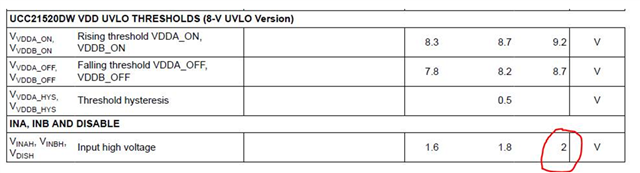
Thank you for your feedback. But still have a question that whether the two input ports can support 3.3V square signal or not? the highest input voltage was 2V,(UCC21520) and 2.3V(UCC21550) but we would input 3.3V , would that be acceptable?

Hi Lillian,
Yes, 3.3V is above the 2V input threshold for "high". The input high voltage should be the same as the input supply voltage.
Best regards,
Sean