This thread has been locked.

If you have a related question, please click the "Ask a related question" button in the top right corner. The newly created question will be automatically linked to this question.

TPS53355: Vout waveform

Part Number: TPS53355

Hi,

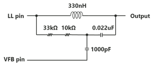
My customer uses the TPS53355 under the conditions of Vin=12V and Vout=1.2V, Iout=0A. In one device, the output voltage became like the waveform in the attached document, and after a while, 1.2V was output normally. I'm thinking that some kind of protection function is working, but could you tell me the cause of this?

TPS53355_waveform.pdf

Best Regards,

Nishie

  • Hey Nishie,

    This looks like a stability issue. I would double check the values of the ripple injection circuit. Can you share the customer schematic?

    Thanks,
    Caleb

  • Hi Caleb-san,

    Thank you for your support.

    I sent you a friendship request to share the schematic. If possible, could you give me your email address?

    The ripple injection circuit is shown below. Using the design tool, I changed the resistance from 43 kΩ to 20 kΩ, but the output voltage waveform did not change. Please let me know if you have any other concerns.

    https://www.ti.com/tool/ja-jp/download/SLURAZ7

    Best Regards,

    Nishie

  • Hi Caleb-san,

    A schematic diagram is attached. I would appreciate your comments.

    6622.Circuit.pdf

    Best Regards,

    Nishie

  • Hello Yuta-san,

    Please allow me till 8/31 to review your schematic and come up with recommendations.

    Thank you for your patience,
    Caleb

  • Hello Yuta-San,

    After taking a look at your schematic I have a few ideas.

    1. Can you make sure that the output is not shorted? The frequency at which the pulsing is happening makes me think that there is a capacitor that is shorted, or maybe a resistor. This can be done by applying a small current in reverse to the output while the device is off. If one of the capacitors is shorted, it will get hot, which you can identify on a thermal camera. You can also double check this by putting a multimeter across the capacitor bank and measuring the resistance.

    2. I would lower the ripple injection resistor to 10kOhms just to see if anything improves, otherwise your ripple injection circuit has no issues.

    3. On the layout, can you confirm that the connections to VBST and the Snubber are not shared through a single via on the switch node?

    Thanks,
    Caleb

  • Hi Caleb-san,

    2. The customer changed the value of the ripple resistor to 10kOhm and saw no change in the output voltage.

    3. The vias are arranged separately. Part of the pattern layout is also attached, so please check it.

    Best Regards,

    Nishie

  • Hey Nishie,

    Layout looks good. Did the customer have a chance to check for a short on the output?

    Thanks,
    Caleb

  • Hi Caleb-san,

    No abnormal heat generation was detected in the output stage. The resistance value was 37ohm to 38ohm. This result is equivalent to a normal substrate.

    The resistance value on the input side is 66kohm to 67kohm for the normal substrate, and 22kohm to 23kohm for the NG substrate.

    Best Regards,

    Nishie

  • Hey Yuta-san,

    I am consulting with a coworker with experience on this device. Please allow me until tomorrow for further recommendations.

    Thanks,
    Caleb

  • Hi Caleb-san,

    Additional information was obtained from the customer.

    After removing the ferrite bead (BF1) from the schematics posted in the past, the output voltage is normal. If you press the FB pin of the DCDC on the front stage of the TPS53355 with your finger, the output voltage is normal. However, the FB1 cannot be removed in the customer's circuit.

    If you have a solution, please let me know.

    Best Regards,

    Nishie

  • Hey Yuta-san,

    A few questions for you. When you remove the ferrite bead do you put a short in its place? And what FB pin are you talking about, the FB pin on the device or the pins on the ferrite bead? 

    Next I ask that you ask the customer to verify the location of C15, we are wondering if the location of this cap in relation to the VDD pin may cause issues.

    Also, can you ask the customer to measure VIN at a cap that is closest to the device, preferably with a differential probe? It looks like the scaling is off on the initial VIN oscilloscope screenshot you sent, so we are wondering if this was an error. Can you provide a screenshot of the VIN caps in relation to the VIN pins as well?

    Thanks,
    Caleb

  • Hi Caleb-san,

    Thank you for your reply.

    A few questions for you. When you remove the ferrite bead do you put a short in its place?

    ->When the ferrite bead was removed, customer put a short in its place.

    And what FB pin are you talking about, the FB pin on the device or the pins on the ferrite bead? 

    ->The FB pin is the FB pin of DCDC that generates 12V.

    Next I ask that you ask the customer to verify the location of C15, we are wondering if the location of this cap in relation to the VDD pin may cause issues

    ->I would appreciate it if you could check the attached pattern layout regarding the position of C15.

    TPS53355 Pattern Layout.pdf

    Also, can you ask the customer to measure VIN at a cap that is closest to the device, preferably with a differential probe? It looks like the scaling is off on the initial VIN oscilloscope screenshot you sent, so we are wondering if this was an error. Can you provide a screenshot of the VIN caps in relation to the VIN pins as well?

    ->I will check the Vin.

    Best Regards,

    Nishie

  • Hey Yuta-san,

    I cannot find C15 on the layout you shared, it looks like VDD is connected directly to the VIN pad without its own filtering resistor. This may be the issue. Can you explain the discrepancy between layout and schematic?

    Thanks,
    Caleb

  • Hi Caleb-san,

    I apologize for the difference in pattern layout numbering from the previously shared circuit diagram. C15 is the same as C452. The red frame in the figure below represents C15.

    Best Regards,

    Nishie

  • Hey Yuta-san,

    This may be a reason that the device is unstable at no load. The VDD capacitor is required to be as close to the device as possible in order to effectively filter out noise. The VDD pin is the input supply for the device controller circuitry. Can you ask the customer to somehow bridge a capacitor near the pin to ground?

    Thanks,
    Caleb

  • Hi Caleb-san,

    Thank you for your reply. I will tell the customer to verify it.

    Best Regards,

    Nishie

  • Hello Yuta-san,

    Understood.

    Thanks,
    Caleb