Hi TI engineers,
There is a high side IC TPS2HB35AQPWPRQ1 in our design,this is the first time for us to use this chip So can you review the schematics for us?
This thread has been locked.
If you have a related question, please click the "Ask a related question" button in the top right corner. The newly created question will be automatically linked to this question.
Hi TI engineers,
There is a high side IC TPS2HB35AQPWPRQ1 in our design,this is the first time for us to use this chip So can you review the schematics for us?
Hi Yepeng,
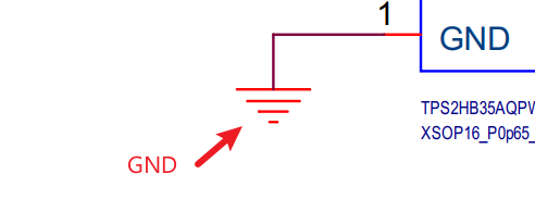
1. I notice that there is no GND network used here. Is there upstream reverse current protection? The device requires a GND network to support the reverse polarity event if there is no upstream protection.
2. I noticed that EN1 and EN2 do not have protection resistors. Please add the protection resistors to these rails.
3. The maximum current that can exit the SNS pin during a fault is 5.3mA and so the voltage could reach 5.3V on the SNS pin. Please make sure the ADC is capable of handling this votlage.
Thanks,
Shreyas
Hi Shreyas,
Thank you for reply!
1. I don't understand what no GND network means, this symbol represents the GND network in the schematic diagram
2. I will add the protection resistor to EN1、EN2 net
3.Thanks for reminding me, I will add a divider circuit to the ADC network
Hi Yepeng,
Please view section 9.3.1.5 in the datasheet for more information about a GND network. This is a diode in parallel with a resistor that connect between the IC ground and the module ground to allow the device to survive negative voltage events like reverse battery.
Thanks,
Shreyas