This thread has been locked.

If you have a related question, please click the "Ask a related question" button in the top right corner. The newly created question will be automatically linked to this question.

LM5146-Q1: Why different MOSFETs for low-side and high side on synchronous buck converter

Part Number: LM5146-Q1
Other Parts Discussed in Thread: LM5146

Hi!

I am designing buck from 75-40V (avg48V) to 36-5V (digipot trimmable) 8A load

I want to use two gan3r2-100cbe for high and low side.

But what's confusing me, is that I see in each ev board design (also webench):

Lower Rds and higher Qg for high side

And higher Rds and lower Qg for low side.

I tried to find why and didn't succeed. Only reason I see is cheaper design.

And probably it is also about Ton Toff sequence.

Can You explain me?

Basic question: may I use identical MOSFET for high and low side?

Should I care about Ton Toff, or controller does itself? 

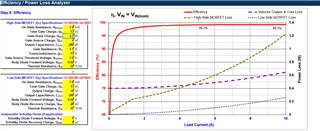
My main goal is highest effecient design because of thermal requirements.

I see that the lowest Qg and Rds I have the better is efficiency.

Stas

  • Hello Stas,

    The lower the RDS on the higher the Qgtotal will be.  There is an inverse relationship between the specs .  Its the same principle as if you were to parallel two MOSFETs, where by the RDS on will half and the Qgtotal will double.   

    Regarding your question about what to select.  As an example, if your VIN was 2X your VOUT, D = 0.5, you would pick RDS on to be the same.  This is because the HS and LS MOSFETs are conducting for the same period of time.  Picking the lowest FET with the lowest Gate charge will typically yield the lowest losses and the highest efficiency.

    For a higher step down ratio you would proportionally pick a higher RDS on for the HS MOSET compared to the low side MOSFET to trade off Rds on for Qg.  

    Please see a application note that goes into detail about MOSFET selection for a buck.

    https://www.ti.com/lit/an/slyt664/slyt664.pdf?ts=1693837119158&ref_url=https%253A%252F%252Fwww.google.com%252F

    Hope this helps.

    David

  • Thank You so much for answer.

    In my application there will be trimmable output voltage IN:50V OUT:36-5V 10A.

    My duty cycle can go from 0.1 to 0.8

    IMPORTANT: I also found out, that LM5146 is not fgood with GaN transistors, because usually they have Vg max=6-7V, but LM5146 is 7.5V output drive.

    So I give up with GaN (even they have the best Qg and Rds).

    Now the best efficiency/ power loss on MOSFET i get on this MOSFETS: ISC0805NLSATMA1 Rds=7.8 mOhm, Qgd=4.7 nC

    I will put these MOSFETs on high and low side, seems like the best solution I found on the market with Rds/Q tradeoff

  • Hi Stas,

    Thanks for using E2E. If you have any further inquiries please reopen the thread.

    Regards,

    Henry