This thread has been locked.

If you have a related question, please click the "Ask a related question" button in the top right corner. The newly created question will be automatically linked to this question.

TPS2663: TPS26631 RPP issue: BGATE not driven high

Part Number: TPS2663

I need some help understanding why a TPS26631 would not drive BGATE high.

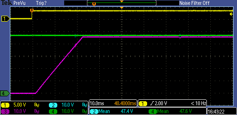
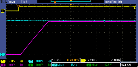
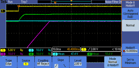
On a single board with 10 independent TPS26631 channels (operating at 48VDC) , only one channel works properly. The other channels do not drive BGATE or ILIM above the input voltage. Consequently the RPP blocking FET is not turned on, and we have lots of heat due to its reverse diode voltage drop. It looks as if BGATE is simply not driven high. There are no board shorts or other explanation I can find. All of the channels are on, power is being supplied out the output, but BGATE is sitting at IN_SYS. Except on one theoretically identical channel which functions perfectly.

On this board, on the failing channels, neither BGATE or ILIM is driven above IN_SYS. FAULT is not being driven low, it is sitting at 3.3V. Power is on and flowing through the TPS26631. Everything appears perfect except BGATE.

I'm grasping at straws on this, so any advice is appreciated.

Details follow.

Thanks in advance.


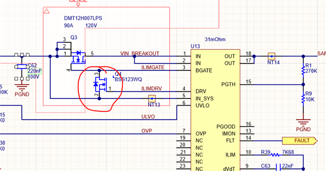
The schematic for a single channel is:


The layout is:

  • Hi Hedley,

    Please share a waveform showing VIN,VINSYS,VOUT,SHDN,BGATE,DRV. It could be external signal is making SHDN pin low. 

    Regards

    Kunal Goel

  • Hi Kunal,

    Thanks for taking the time to give this a look. I don't have a great scope (DPO2024), and it's a bit out of cal, but here you go.

    This is for a channel that is not working. The output is driving a 22 Ohm resistor.

    Yellow is SHDN. Pink is VOUT. Green is VIN_SYS, and Blue is VIN (pins 1&2).

    In the above shot, you can see that output comes on as expected when SHDN rises. You can also see that both VIN, and VIN_SYS are high throughout and if you squint a bit, you can almost make out that VIN is ever so slightly higher than VIN_SYS. This scope's measurement function leaves a bit to be desired, however, the mean measurements of channel 2 (VIN) and channel 4 (VIN_SYS) would seem to indicate that the pass transistor is not on.

    Ok, so the next two shots are looking at BGATE (green) and DRV (blue). They are both from the same edge of SHDN event, the difference is whether the Green or Blue are in front, and that is just to basically show that they are pretty much at the same voltage (neither is turning on a FET).

    I went back and grabbed a shot from the one working channel on this board. 
    In this shot, yellow and pink are still SHDN and VOUT. Green is BGATE, and blue is VIN_SYS.

    Here, it looks like BGATE sits at VIN_SYS until SHDN rises. Then BGATE rises in about 4ms to about 10V above VIN_SYS.
    I remain entire confused as to why this channel functions properly, but the others don't.

    Thanks,

    Hedley

  • Hi Hedley,

    1. For all the channels VIN and VOUT is independent? I mean no short among VINs or VOUTs

    2. Exactly same schematic for all channels?

    3. It is possible that this DRV FET is showing some issue on other channels and because of which VINSYS and BGATE are getting shorted?

    Regards

    Kunal Goel

  • Hi Kunal,

    Had some vacation, so sorry for the long delay.

    All channels have independent VINs and independent VOUTs and have exactly the same schematic. It should have been mentioned that we are attempting to modulate some data on the VIN (2-4 volts), and this modulation is likely the culprit of the problem as it lowers VIN briefly.

    Management decided to rip these two transistors out because they are not absolutely required for our application, and we need to move forward. So while we do not have a NP complete proof of exactly what was happening, this issue can be considered to be resolved. 

    Thanks for the help and thanks for being there.

    Hedley