This thread has been locked.

If you have a related question, please click the "Ask a related question" button in the top right corner. The newly created question will be automatically linked to this question.

UCC28070: Schematic review

Part Number: UCC28070
Other Parts Discussed in Thread: TL431

Hi team,

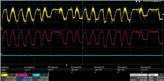
My customer shows the waveform as below. pls help check the schematic. thanks

the waveform is BD+ when PFC has no load. 

3821.PFC.pdf

  • Hello Jimmy, 

    Thank you for your question on the UCC28070 controller. 

    The above screen-capture has two waveforms.  I assume that Ch2 (red) is BD+ and Ch1 (yellow) is VINAC (with switching noise superimposed on the signal).  

    Since the test condition is at no load, there is not continuous switching.  Instead there may be scattered random bursts of switching her and there, not necessarily on both outputs GDA and GDB.  This is normal behavior because the VAO voltage is down near the 1-V threshold for switching.  

    Because the switching is random, the pi-filter capacitors FC1 and FC3 are peak-charged to the peaks of the input AC line.  When there is no switching, there is no inductor current to pull down the voltage on these caps, so the voltage appears to stay flat.  When VAO rises above 1V and switching happens, some current is pulled out of FC1 and FC3, so their voltage follows the AC line wave shape down.  If switching stops the voltage will stay at the level it was at when the switching stopped.  If switching resumes, the cap voltage will fall further toward the zero-crossing, otherwise, it will follow the AC envelope back up on the next 1/2-cycle.  

    So the waveform may look a little "ugly", but at no-load this is normal.  Add a little load and this will clean right up because VAO rises sufficiently above 1 V to maintain continuous switching. 

    For schematic review, the main issues I found are:
    1.  I could find no connection between PGND of the power stage and GND of the controller. 
    2.  The return paths of current-sense transformers TR1 and TR2 (through RT1 and RT2) should go to GND at the IC, not to PGND.   Route these returns as a signal-pair with CSx.
    3.  Current-sense diodes D6 and D* should not be schottky diodes.  Too much junction capacitance.  Please change them to P-N types, like D5, D7. 
    4.  In my opinion, the gate-drive networks for Q1-Q4 are more complicated than they need to be. 
    5.  The value of R49 on IMO pin has two "K"s.  I'm sure the value shouldn't be 10Meg.   
    6.  C7 and C8 values can be 10~20x higher.  I suggest 50~100us time constant for filters on VSENSE and VINAC. 
    7.  I see that L1 and L2 are separately-fused inputs at the AC-line.  I presume only one input will be connected at a time, not both at once.  
    8.  TL431 (U6) at Inrush Relay can only drive its cathode voltage to 2V, not to 0V, so FET Q9 may not fully turn off.  Please check this operation.  Also, consider to increase C29 value a lot to improve noise immunity. 

    Regards,
    Ulrich

  • Hi Ulrich,

    Thanks for your help. so if when no load, the BD+ waveform will different on every production board?

    If I use BD+ signal to flyback controller as a brown out signal. 

    Because the no-load signal of each board is different, the function of undervoltage protection will be abnormal. What do you suggest?

  • Hello Jimmy, 

    As you can see with the red waveform above, the BD+ signal will be different from one cycle to the next, regardless of one production board or another. 

    If your flyback controller detects brown-out by sensing the peak BD+ voltage, then you can still use this signal at no-load because BD+ never exceeds the peak of the input line.  Most brown-out detectors have a time delay (such as 60~100 ms) before activating the brown-out response.  The BD+ signal may add 10~20ms more delay because you have to wait until some PFC switching pulls the BD+ voltage down to a lower level to detect a possible brown-out. 
    If that is acceptable, then no design change is needed.  You can verify the function by testing at light-load, then at no-load. 

    If brown-out is detected in some other way, then maybe the best solution is to add two new diodes (such as 1N4006 or equivalent), one anode to L, one anode to N, and both cathodes together to provide a separate "BD++" signal without any capacitance after the diodes to hold a charge.  Some pull-down resistance on BD++ will be necessary.  These can be D14 and D15 in your schematic, for example.  

    Regards,
    Ulrich