This thread has been locked.

If you have a related question, please click the "Ask a related question" button in the top right corner. The newly created question will be automatically linked to this question.

TPS51116-EP: High Frequency Operation at 1.8A

Part Number: TPS51116-EP
Other Parts Discussed in Thread: CSD17304Q3, TPS51116

I am using the TPS51116 in DCAP mode for a 1.35V output. I am using Rds_on sensing, with a high/low-side TI CSD17304Q3 FET.

I am seeing unusual behavior of the part at around 1.8A output. Below 1.8A the part operates normally. When I first observed this behavior, I increased my RTRIP resistor thinking the part was in OC limit, but even after I increased the resistor to increase the OC limit, the part still shutdown at 1.8A again.

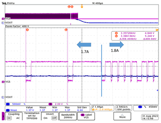
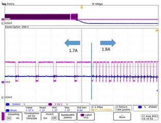
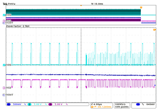
The scope capture below (Vgs low-side FET in pink, Vout in blue) shows the part operating normally at around 400kHz switch frequency below 1.8A. When the load current is beyond 1.8A, the switch frequency increases to about 2.2MHz. I didn't think the part would go into a 2.2MHz operation, with the normal frequency set around 400kHz.

I also captured the LL pin (i.e. switch node in teal) since this doubles as the current-sense point when using Rds_on sensing. The switch node appears to be oscillating which lines up with the time that the Vgs increases in frequency. I have a snubber R and C on the switch node if there is some sort of oscillation occuring, but I do not see how going to a higher output current would cause this oscillation when at lower load currents the oscillation would occur.

Does the DCAP mode need to sense the inductor current mode when using Rds_on sensing? I am wondering if I should change my low-side FET to a part with higher Rds_on to get more signal for sensing the inductor current. I am not sure why the output would work a lower currents with less signal and then start shutting down at higher currents when there is more signal at the LL pin, but it was just an idea if the output is going unstable.

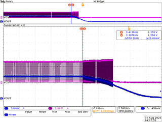
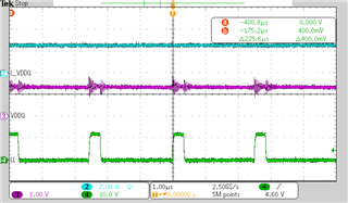
The final scope capture shows the 1.35V output slowly dropping to zero when I step the load to 1.8A.

Has anyone seen this behavior before?

  • One thing I have noted for the feedback resistors to generate 1.35V:

    My current values are 6.04kohms for the high-side resistor and 7.5kohms for the low-side resistor into VDDQSET. Some other schematics I have seen (including in the datasheet) have 10x these values, such that the low-side resistor is 75kohms and 60.4kohms.

    Since DCAP mode relies on a certain amount of ripple to determine on and off time, would this be a possibility for the issue I am seeing?

  • Hi Timothy,

    Can you share your schematic and layout for reference?

    You can try raising the resistor values as you mentioned but on the EVM schematic, the resistors used are both 4.75k so I don't think the values you have in your design are unreasonable.

    Regards,

    James

  • I am trying to see if I am able to share my schematic/layout for reference based on my company's IP policies.

  • James,

    I am looking at my artwork and I found that my note to our PWB designer was missed regarding tying the thermal pad to PGND underneath the package. Do you know what would happen if PGND is tied to the thermal pad right underneath the part? I am wondering if I have a noise issue with my layout.

    The eval board has this pin tied to the rest of the GND plane and the thermal pad underneath the part on an internal layer.

  • Hi Timothy,

    There's a section in the datasheet regarding layout considerations that specifies not to connect PGND directly to the thermal pad under the device if I understand this correctly. Considering that this is a bolded statement I would make sure PGND is connected to an internal GND layer rather than at the thermal pad under the IC. This could be a noise related issue just based on the scope captures you shared. It looks like there's some slight positive feedback going into the switching waveform before the device fully fails.

    If I can get a scope shot of 1.8A operation using our EVM I will share that here but I would start by addressing the PGND issue.

    Regards,

    James

  • Hi James,

    Agreed that the PGND pin should not be tied to the thermal pad under the device. I originally gave this note to our PWB designer who implemented it, but after the board was released it looks like keeping PGND separate from the thermal pad was not followed.

    I will try to do some testing to isolate PGND from the thermal pad and tie it directly to the low-side FET source pin (since this design utilizes Rds_on sensing). Maybe that will clear up the issue. Stay tuned,

  • Hi Timothy,

    Sounds good, let me know what you find.

    Regards,

    James

  • Hi James,

    I ended up isolating the PGND pin from the thermal pad, but I am still seeing this issue, with the output shutting down at 1.8A.

    My question is regarding the GND pin. How should this pin be laid out in the design. In the eval board, it is tied directly to the thermal pad underneath the part, but theoretically there should be no current flow in this area.

    My GND pin does connect to this thermal pad on Layer 1, but it may or may not be isolated from higher current noise. I am not sure if that is causing the issue. I am trying to perform a test to isolate the GND pin and see if the shutdown still occurs.

    Any other thoughts on this though?

  • Hi Timothy,

    A couple other things to check:

    • What's the value and saturation current of your inductor?
    • What are the values for your RC snubber? The layout recommends 3Ohms and 1-nF so I would just like to confirm those values.

    The GND pin should be connected to the negative terminal of the VTT LDO output capacitors. On the EVM this is accomplished with the 4 vias just below the IC pad. These vias connect both the VTT LDO output capacitor negative terminals and the GND pin to the next GND layer. In this sense the GND pin should be connected to a large, stable GND reference.

    I can check the EVM behavior and let you know what I find at 1.8A as I mentioned before. I should have some data to show by Wednesday.

    Regards,

    James

  • The inductor is 2.2uH, with a saturation current of 12A.

    I do have the RC snubber in the design, but not populated. I could try installing those, but I do not see a lot of ringing on my switch node, which looks pretty clean. The values I have are 3.01ohms and 1nF. I could try installing them to see if it helps.

    One thing additional to note: I am getting the output to shutdown when I probe with my finger on the GND pin. This test adds some capacitance to that node to see that it is sensitive, and the output will shutdown when I probe this pin with a long lead and my finger touching the lead. I connect the GND pin right to the thermal pad, just like the eval board, but maybe I have too much noise on this pin and it is causing the output to shutdown.

    I may try to lift the lead of the GND pin and route it somewhere less noisy, but again I followed how the eval board connected the GND pin.

  • After looking at the Eval board, it looks like there are more than just 4 vias that connect the GND pin to the internal plane. There are 3 additional vias that tie in all of the GND planes on Layer 1 -4. I highlighted them below.

    I would have thought that the VDDQSET FB resistors would have been tied to the GND pin, but instead they tie to the VTT LDO output capacitors and then tie to GND with the vias you just discussed.

  • Hi Timothy,

    Try populating the snubber and see if that fixes the issue. In the layout guide this snubber is described as a preventative measure for "high frequency surges". In my mind a surge is a bit different than what you experience at 1.8A, but perhaps the snubber will add some stability in this regard.

    Usually, emulating the EVM layout is a good option when debugging problems. If you have extra room to add more GND vias under the IC to connect the GND pin to all internal layers, this may be something to add.

    Regards,

    James

  • Hi James,

    I populated the 3ohm and 1nF RC snubber, and I was able to regulate beyond 1.8A. However, the output shutdown at 2.4A this time. Maybe the RC snubber helped with some of the noise, but at the higher currents it still caused the shutdown.

    Again, I am seeing the controller switch node switch from the nominal 400kHz frequency to 2.5MHz.

  • I also lifted the GND pin and connected it to a "quieter" area of the board and I am seeing no change in performance, with the output still shutting down,

  • Hi Timothy,

    I did a bit of testing on the EVM and grabbed the below scope captures. I'm able to source up to 2.8A from VDDQ without experiencing a shutdown. Increasing the load current increases the output ripple but does not trigger a fault condition.

    I am measuring LL from the bootstrap capacitor to the nearest GND point on the EVM, which is C1 GND terminal when looking at the schematic in the User's Guide. I am using the tip-and-barrel method of probing to reduce the interference from the probe.

    Capture showing VDDQ operation as load increases from ~200mA to 2.8A (12V VIN)

    Capture showing VDDQ operation at 2.6A, zoomed in to show 400kHz stable switching speed (12V VIN)

    Questions I have going forward:

    • I have VDDQ set to 1.5V in these tests. How are you achieving 1.35V in your design? I may be able to modify the EVM to test again at 1.35V.
    • Were you cleared to share either the schematic or layout? If not, can you describe the main differences between your schematic and the EVM? You may want to try using the same output filter and compensation components shown in the EVM as a test. I'm a bit limited in my recommendations without a schematic / layout.
    • Have you checked your OCL settings using Equation 5 in the datasheet (Under the section titled "Current Protection for VDDQ")? What value are you using for your RTRIP resistor?

    Regards,

    James

  • James,

    Unfortunately, I am not able to share artworks or schematics, so there may not be more else to this thread without you being able to review those.

    I do think that I have narrowed my issue down to a noise issue related to PGND noise coupling into the controller. I have a mod with the PGND pin routed directly to the FET source and that seems to help.

    Would it be possible to get one of the eval boards sent to me, or would I need to order one of those from the TI website? Didn't know if those eval boards were considered samples.

    I modified the design by using FB resistors into the VDDQSET pin. you should be able to do this on the eval board. My resistors are 6.04k and 7.5k.

    I have the OCL resistor set much higher than the 1.8 / 2.4A shutdown that I am seeing, so I do not believe it is related to that.

    Thank you for the help.

  • Hi Timothy,

    For EVM access you would need to order one from the TI website. I can use the one I have here and see if I can swap the VDDQSET resistors to make sure the operation doesn't change under this condition.

    It sounds like this issue is noise related from your description of the PGND modifications. In general, making sure the high current switching loops are as small as possible is a good way to prevent EMI. It can also be beneficial to match the loop sizes.

    Regards,

    James