This thread has been locked.

If you have a related question, please click the "Ask a related question" button in the top right corner. The newly created question will be automatically linked to this question.

LM5113: DCDC 1/4 1000W converter

Part Number: LM5113
Other Parts Discussed in Thread: LMG1205, LMG1210, LMG1205HBEVM, , LM5017

Dear TI support team,

We are currently on a stage of firmware development for our own DC/DC converter based on dsPIC33CK256MP202. I’m using simple project code based on data sheet example “High-Resolution PWM with Fine Edge Placement” p.123, 5.3 Simple Complementary PWM Output mode. During FW testing on the device, I’m observing short on transistors on PWM1H part of the circuit, after that I can’t move forward of the development process.

Our project based on https://epc-co.com/epc/products/demo-boards/epc9143 1
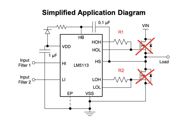
Drivers: LM5113SD
Transistors: EPC2306 High side, EPC2302 low side.

Technical parameters: Voltage input: 36…58V Voltage output: 10.8…13.2V Rated power: 1000W Output current: 85A Quantity phases: 2 pcs Protection: UVLO, OVP, OCP, OTP Frequency: 500 kHz Type topology: Synchronous Buck DSP controller: dsPIC33CK Type transistors: GaN

We have some discussion with Microchip support, they suggest to ask TI support..

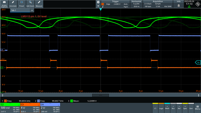
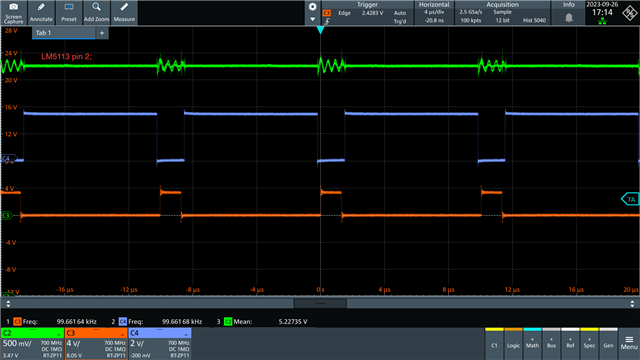
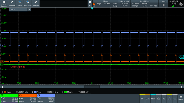
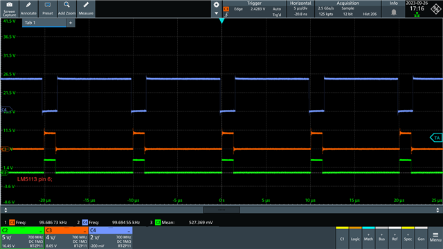
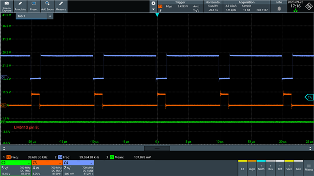
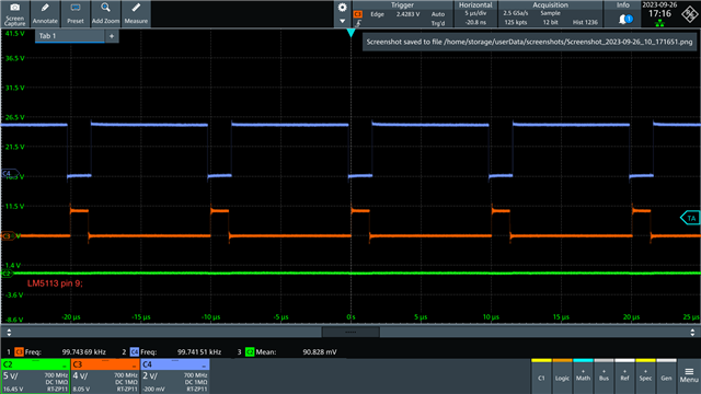
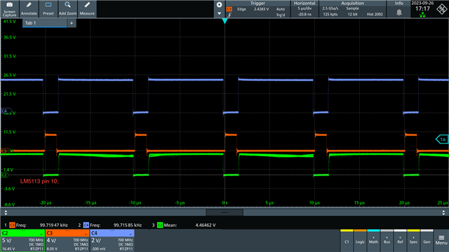
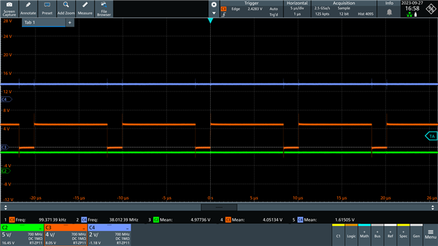
During debug process, I unsoldered transistors and after that I can safely observe waveform on oscilloscope, please find photo in attachment.

green/yellow input from dspic33 to driver, blue and red output from driver to transistors gates.

Some additional info about debug process:

We connected constant voltage power supply to 12V brick output pins in order to put 12V on it's output and check waveform from drivers output.

  1. It goes to constant 12V, straight line, no PWM from LM5113SD,
  2. Then we tried to decrease voltage level on power supply and after that we observe that PWM signal becomes normal when we have 1.4V from power supplier.

Please help to find solution, Thank you.

  • Hey Nikita,

    Thank you for your question regarding the LM5113.

    Can you please provide the schematic for this setup so that I can investigate further?

    Let me know if you have any other questions.

    Thank you,

    William Moore

  • Hello William,

    Is it possible to setup NDA for that purpose?

    Have a nice day,

    Nikita

  • Hey Nikita,


    1. Do you have a TSR or FAE to set up an NDA? They are typically the ones that handle that.

    2. Have you replaced the driver with a known good part and had the same results?

    3. How many did you boards did you build and how many of those had issues?

    By looking at the EPC9143 Schematic, it differs some from the Functional Block Diagram in Section 7.2 from the LM5113 datasheet that can be found at this Link. The EPC9143 does not include a bootstrap diode or resistor from VDD to HB that I can see and you would need to include that in your circuit.

    Let me know what you have done thus far and if you have any further questions.

    Thank you,

    William Moore

  • Hey Nikita,

    Were you able to find a solution for this? If so, could you share your findings?

    Thank you,

    William Moore

  • Hello William,

    Sorry for late reply.

    1. I could handle it, no problem. If it's possible to navigate me to the right person, please help here.

    2. Yes we did, certain amount of iteration and we have got same results.

    3. Every board.

    According to: "The EPC9143 does not include a bootstrap diode or resistor from VDD to HB that I can see and you would need to include that in your circuit."

    We tried this. No success.

    Thank you,

    Nikita

  • Hi Nikita,

    William is out of the office for a couple of days and will be back Monday. He should respond to you when he is back in office.

    Regards,

  • Hey Nikita,

    Sorry for the delay with me being out of office.

    With this device, we have seen that the clamp circuit sees the high voltage on HB-HS on startup as being overcharged and it opens the bootstrap path so that it can't charge the capacitor. A possible solution is adding the bootstrap circuit and using a high resistance (possibly >20 Ohms) bootstrap resistor so that it cannot overcharge realistically unless HS is held negative.

    Another option is the newer LMG1205 that is very comparable in specifications and it integrates the bootstrap diode.

    Let me know if there are any further questions.

  • Hello William,

    Thank you for your response. Will try solution with  LMG1205

  • Hello William,

    Is there any possibility to find analog of LMG1205 in WSON-10 package?

  • Hey Nikita,

    We do not have a half bridge driver in the WSON-10 package or have any planned for the near future. You could consider the LMG1210 as well for a half bridge GaN driver, but it is not WSON-10 either. We do offer other GaN drivers that are low side only if you would consider taking a look at our portfolio there.

    Let me know if you have any further questions.

    Thank you,

    William Moore

  • Ok, got it.

    So, for testing purpose (in order to test existing pcb boards, that we have on hands) it could be better to try https://www.ti.com/tool/LMG1205HBEVM, does it?

    1. Unsolder LM5113SD

    2. Connect PWM signal from Microchip controller to LMG1205HBEVM

    3. Connect output from EVM board to EPC transistors gates


  • Hey Nikita,

    Trying to use the LMG1205HBEVM is okay for testing purposes but there is not much guarantee that this will work well due to when working with GaN FETs the layout of the PCB is very crucial for optimal operation. So, you may see some unfavorable conditions by testing it this way.

    As a reminder, using the LM5113 does work, but when implementing the bootstrap diode you need to also include a bootstrap resistor of relatively high value (>20 ohms) to make it work. This may be a possible test case before having to make any major changes.

    Let me know if there are any further questions.

    Thank you,

    William Moore

  • Hello William,

    According to bootstrap resistor. We soldered 20Ohm resistor sequentially to bootstrap diode. Transistor was successfully burned.

  • Hey Nikita,

    I am still investigating this and will get back with you on the findings but I just want to confirm, are you using the LM5113 or the LM5113-Q1?

    Currently, the LM5113 is not recommended for new designs as indicated on ti.com, but the LM5113-Q1 is still listed as an active part. So, I would recommend using the LM5113-Q1 over the LM5113 if you are looking to stay with that series part and not transition to LMG1205.

    Let me know if you have any further questions.

    Thank you,

    William Moore

  • Hey Nikita,

    Also, a couple further questions.

    1. Is the driver itself failing or is it just the GaN FETs?

    2. Can you please measure the voltages on each pin of the driver and send us waveforms? We need to ensure that none of the recommended operating specifications are violated. Also, when taking these measurements, ensure that the ground loop is as short as it can be.

    Let me know if you have any further questions.

    Thank you,

    William Moore

  • Hello William,

    We are using LM5113, as far as I can see on chip, it says L5113 no additional info.

  • William,

    1. I'm not sure about driver.

    2. Please see attachment. Pay attention that I can safely observe waveforms only if Hi/Lo side resistors unsoldered apart of transistor gates.

  • Hey Nikita,

    If the LM5113 is not failing, you may be having a problem with overvoltage/overcurrent of the FETs and that would need to be investigated by EPC. With this uncharacteristic VDD and the rippling on HB and HOH, that could be the OV/OC on the FETs and causing the failure.

    There is too much low frequency noise on VDD of around 0.5V. Please ensure that the VDD capacitor is as close to the IC as possible and large enough. The sizing of this is explained and shown in section 8.2.2.1 in the datasheet for VDD Bypass Capacitor.

    If both of the GaN FETs are failing, then your deadtime may be too short because in some operating conditions, the deadtime gets sacrificed which kills the power devices.

    Can you check these things and let me know your findings as well as the deadtime and bypass capacitor that you are using?

    Thank you,

    William Moore

  • Hello William,

    On some of the iteration we fixed this low frequency noise on VDD by adding external capacitor to +5V circuit (we are using LM5017 in order to convert 54V to 5V). Today I repeated all steps. And here is behaviour:

    1. Transistors complitly unsoldered.

    2. 5V Stabilised, no low frequency noise on VDD.

    3. After power on, 10 seconds left we observe no PWM signal on Hi side. See video.

  • Hey Nikita,

    Unfortunately I cannot view this video. Can you send waveforms images of this new setup with the FETs in and a stabilized VDD? With the FETs out, we cannot get an accurate representation of what is going on.

    With this VDD noise and the driver not failing but the FETs are, then this could be an issue with the FETs that would need to be taken up with EPC. With the waveforms that you previously sent, only the VDD waveform is really a problem, so if you can get the VDD signal clean with the capacitor, then you could likely solve your problem.

    Let me know what the results are that you get from this.

    Thank you,

    William Moore

  • Hi William,

    Please refer to the screenshots. After 10 seconds we observe no PWM signal on High side.

    Blue - hight side

    Red - low side

    Green - 5V level

    If we will connect transistors to the board with such PWM it will be burned, indeed it was.

  • Hey Nikita,

    With no FETs installed, the switching node (HS) has no path to ground during the low side ON state and therefore it cannot charge the bootstrap capacitor. So, the 10s of operation you see is just how long it is taking the bootstrap capacitor to discharge and continue driving the high side.

    The biggest concern that I see with your overall setup is that you need to clean up the supply voltage waveforms.

    Let me know if you have any more questions regarding this.

    Thank you,

    William Moore