This thread has been locked.

If you have a related question, please click the "Ask a related question" button in the top right corner. The newly created question will be automatically linked to this question.

UCC27223: Relationship between C2, D1, R1, and C1

Part Number: UCC27223

Note: the component designations that I am referring to in this post come from the data sheet of the UCC27223

I am monitoring the VLO voltage (on C2) under changing load and input voltage conditions.  What I am finding is that under high output load and high input voltage, the VLO voltage drops below 3.9V, which is triggering an UVLO condition.  I have confirmed that the input voltage to pin 3 (VDD) is not dropping too low, and I have put 3x 10uF ceramic caps in parallel right next to the UCC27223 so that the input voltage stays steady under load.

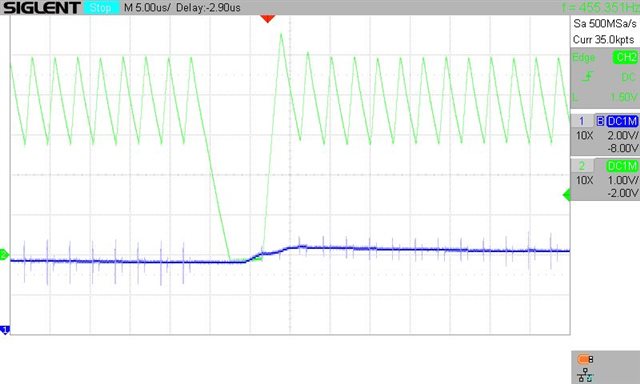
I think there is something that I do not understand about the generation of VLO inside the IC.  Here is an image of what is happening:

Ch1 (blue) VLO signal.

Ch2 (green): output current waveform, around 4A RMS in this example

- VLO has a slow decay, and when it drops to around 3.9V, the UCC resets.  When there is no load, VLO pops back up to around 4.2V and the UCC restarts.
I have experimented with different current ratings of the Schottky diode D1 (1A vs 3A).  This does not have any effect.

I have changed the value of the VHI resistor R1.  0 Ohms is the worst - the reset occurs at around 4A RMS output as shown in the image above.  When R1 is changed to 4.7 Ohms, the output current can be increased to around 6A RMS before the UVLO reset occurs.  Increasing R1 to 10 Ohms does not offer any improvement over 4.7 Ohms.  For reference I have included a table below showing the various FET's that I am experimenting with.  All have fairly low/fairly similar gate charge specifications.

Reducing the value of C2 from 2x1uF MLCC to a single 100nF capacitor definitely makes the problem worse: in this condition the ULVO triggers at around 2A RMS output.

I have experimented with different values of C1, from 100nF to 220nF but this shows minimal improvement.

What I find curious is that at a given output current level, say 5A RMS for example, if I increase the input voltage from 14V to 17V in 1V increments, the UVLO reset gets worse.  At 17Vin, the load has to be dropped to 3A RMS to keep the UVLO from triggering.  If I reduce the input voltage to 12V, then I can increase the output current to 6A RMS and UVLO does not trigger.  When I bump it up to 7A then UVLO will start to trigger.  

The UCC27223 data sheet says that C2 should not be more than 4.7uF.  At this point I need some guidance as I think that the issue may be a combination of values for C2, C1, R1, and D1 for the target FET's that I am using.

For reference: 

Vin: 10-17V
PWM input is coming from a hysteresis-drive circuit (output is a current source).  I am sensing the output current with a INA180A2 fed into a high-speed op-amp to create the PWM Input signal for pin 7.  I can share the schematic if you send a private link to me.

The operating frequency is around 300-350kHz.  The frequency varies with load and Vin.  I would like to move to a higher frequency if there is an improvement in efficiency.

Thoughts?

  • Hey Jeff,

    Thank you for your question regarding the UCC27223.

    I have just a couple questions to try and provide support for this.

    1. Where in proximity to the driver are the CIN, C1, and C2? These need to be placed as close as physically possible to the driver.

    2. It appears that you are near the right range for values for C2, C1, R1, and D1. There is guidance in the datasheet on the selection of these values with equations. What value are you using for CIN?

    3. Can you send the schematic and layout over so that I can review those? If that isn't something that you want posted publicly. You can add me as a friend on here and we can continue this discussion via email.

    Let me know what you gather from this and if you have any further questions.

    Thank you,

    William Moore

  • For the edification of other interested parties I will share what I can.  I have also sent a "friend" request so that we can discuss other details privately.

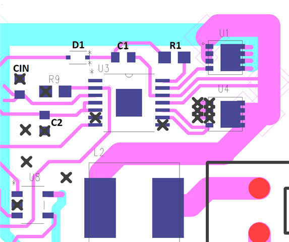
    A snip of the layout is shown below.

    CIN is 3 x 10uF stacked side to side.  U8 is the op-amp that is generating the PWM.  

  • Hey Jeff,

    I am closing this thread as it has transitioned to email. Please follow up if you still need help regarding this either here or through email.

    Thank you,

    William Moore

  • What I found (finally) is that I am using the UCC27223 in an atypical way, as the operating frequency is not fixed.  I am using a hysteresis drive circuit as mentioned previously.  This results in different operating frequencies as the input voltage varies, (higher Vin = lower frequency).  The frequency also drops as the load increases, but not as much.

    It seems that the UCC27223 prefers to operate above 300kHz or so.  I am able to vary the operating frequency (at a given load and input voltage) by changing the gain of my hysteresis control.  Higher gain = higher operating frequency.  By bumping the nominal frequency (at 14Vin) up to around 450kHz, then the frequency drops to around 390kHz at max. Vin (17V).  The higher frequency prevents the "reset" of the UCC27223.  

    I still don't knw what is causing the reset of the UCC27223, as this seems to be an undocumented protection feature.  I added low-ESL capacitors (helped slightly) and increased the amount of capacitance across Vin (helped quite a bit).  It would be nice to know definitively what causes the reset.

  • Hey Jeff,

    I am currently investigating this and will plan to get back with you by the end of the business day tomorrow.

    Thank you for your patience,

    William Moore

  • Hey Jeff,

    So here is what I have found.

    The UCC27223 does not have UVLO on the high side, but from what it appears you are entering UVLO on the low side. One thing to consider with this is that the voltage measured at the pin could be different from what the device internally sees based on the noise and inductance in the bond wires.

    When running at the 300kHz, does the noise on VDD or PGND change as compared to running at different frequencies?

    It seems that this large ripple that you are seeing could be causing an internal reset. This could be taking place on VDD, VLO, VHI, or ENBL. With the improvements with larger capacitance, it leads me to believe that this ripple is occurring on VLO or VHI and causing this problem.

    Increasing VLO and VHI could help in this case as well with the increased capacitance as we have discussed before.

    Can you increase the capacitances on VLO and VHI simultaneously and measure the voltages at the pins to see if the ripple is improved? As well as take scope captures beforehand to see the differences?

    Please let me know if you have any questions.

    Thank you,

    William Moore

  • Refer to the table below.  The last 2 rows show ENBL and VLO voltage under various conditions.  It does appear to be an issue with VLO undervoltage reset.  I have scoured the UCC27223 datasheet for any hints but the document is vague regarding VLO: on page three (top, in the table) it describes a typical voltage of 6.5V for VLO, and then right below describes undervoltage lockout.  However there is no indication as to what would load down VLO to cause the voltage to drop.  I DO see that VLO varies quite a lot in different input voltage and load conditions, and it seems that the combination of high input voltage, high load, and low operating frequency causes undervoltage to trigger.  I would really like to know how to prevent this from happening.

    Index of 20230923 scope waveforms
    R3=100k, R17 = 470
    R3 = 100k, R17 = 2.2k
    PNG file 001 002 003 004 005 006 008 009 010 011 012 013 018
    % duty cycle in. 20 20 20 60 60 60 20 20 20 60 60 60 60
    Vin 10 14 17 10 14 17 10 14 17 10 14 17 17
    Power in 4.53 4.98 5.29 16.92 17.49 18.93 4.81 5.33 5.7 16.94 17.57 18.66 18.3
    freq. kHz 544 453 416 571 487 454 385 381 339 408 392 377 357
    duty cycle % 30 22 18 39 27 23 30 21 18 27 22 22 31
    V ENBL (Ch1) 5.1 5.0 4.3 5.0 3.9 3.3 5.1 5.1 4.4 4.3 3.5 3.5 3
    VLO (Ch2) 6.3 6.2 5.6 6.6 5.1 4.4 6.5 6.6 5.8 5.4 4.6 4.6 3.6

    Component values (using designations from SLUS558 figure 3):  
    Cin
    2 x 10uF + 1 x 0.1uF
    C ENBL (not in Fig 3)
    0.1uF + 360k
    C2
    2.2uF + 0.1uF
    C1 0.1uF
    C OUT none

    - I tried changing D1 to ultra-fast (3nS trr) Schottky: no effect
    - I tried adding an additional 2.2uF in parallel with C2: no effect
    - I tried changing C1 from 0.1 to 1uF: no effect

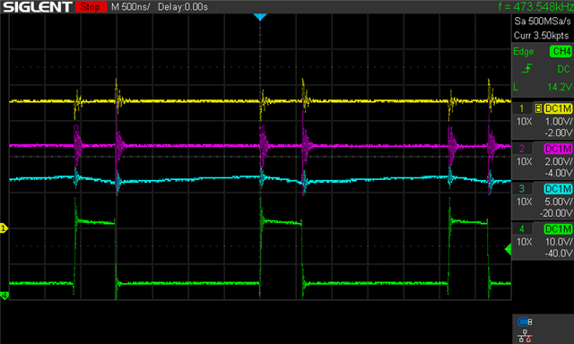
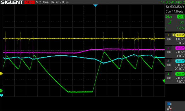
    Below I have attached two waveforms, reference 013 and 018
    Ch1: ENBL    Ch2: VLO    Ch3: VIN    Ch4: VHI

    Note that in the second image (018) I switched Ch4 to a current probe so that I could trigger on the event where the output resets.  There is some ringing in the first image (013), I think that is just my scope setup.  The ringing is not present in the second image (018) because I am no longer connected to VHI.  013 is set up under the same conditions as 018, the only difference is that 013 captures when the output is operating normally and 018 captures the reset event.  You can see that ENBL and VLO are definitely in the "danger zone" per the data sheet.  

    To explain a few things in the table: R3 and R17 are the hysteresis circuit.  This is mostly for my reference but you can see how changing R17 changes the operating frequency..  The reference to "% duty cycle in." is also for my reference - this duty cycle is proportional to the output power.  Also note: the frequency of operation shown in the upper right corner of the images is not always accurate.  I calculated the actual frequency that I list in the table above from the images.

    Here is image 013:

    Here is image 018:

    William, I will send you an email with all of the scope images for your reference.

  • Hey Jeff,

    Thank you for all the scope plots and the data. I did receive your email with all of the files.

    I will be reviewing this and investigating it and plan to get back with you by the end of business tomorrow.

    Let me know if I can be of any further help in the mean time.

    Thank you,

    William Moore

  • Hey Jeff,

    Thank you for your patience.

    Can you try to set this up with a single, large form factor 4.7uF capacitor on C2 as well as using a 0402 capacitor for the high frequency noise filtering on C2 of 0.1uF on C2 as well. Also, increasing Cin as you previously stated that that helped significantly.

    On reviewing some of the correspondence here, with the Rboot resistor, trying a 1Ohm or 2Ohm could provide some resolution. Also, increasing C1 (bootstrap capacitor) would help with the sharp ripple that you are seeing on your waveforms.

    Let me know what the results of trying these suggestions are and if you have any further questions.

    Thank you,

    William Moore

  • I changed C2 to 0603 4.7uF + 0603 0.1uF (I don't have any 0402's).  I made a new board rev. that allows me to add more capacitance across Vin (currently 3 x 10uF 0603 + 0.1uF 0603).  This seems to improve things so I think that I am headed in the right direction.  In previous board revisions I experimented with changing the bootstrap resistor and capacitor (R1 and C1 in Figure 3 of the data sheet).  I could not see any definitive improvement however at that time maybe the problem was related more to Cin and C2.

    I came across the following statement in a different TI data sheet that got me thinking:

    "The value of a ceramic capacitor varies significantly over temperature and the amount of DC bias applied to the capacitor....For this example design, two (10-μF, 50-V, 1206, X7R) capacitors have been selected. The effective capacitance under input voltage of 24 V for each one is 3.45 μF."

    This could explain part of the reason that when I increase the input voltage, the problem gets worse: maybe the effective capacitance of Cin is dropping to the point where the ripple triggers a reset.  I'm going to call it good for the sake of the discussion forum.

    Thank you for your help and all the best...