


Other Parts Discussed in Thread: TPS552882, TPS55288, , TPS55288-Q1
Hi, I have a schematic based on a webench solution which I have modified slightly and I just want to check if everything looks ok. It is for 6-36V input with a 12v 6A output.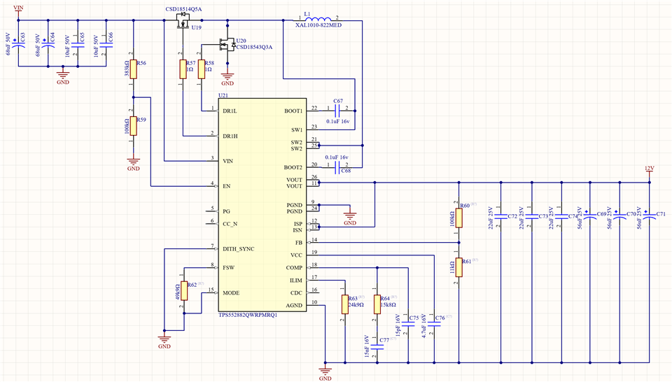
1 question I have is about the input and output capacitors. Are the large aluminium capacitors necessary? I saw on the datasheet that they don't put them in the example application but they are added on webench. I have this as this power feed which supplies the VIN input to this circuit:
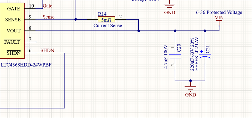
It already has a large 220uF capacitor. Can I change the aluminum ones on my buck-boost?
Thanks all!


 3D
3D Top Layer
 L2 - GND
 L3 - Contains AGND
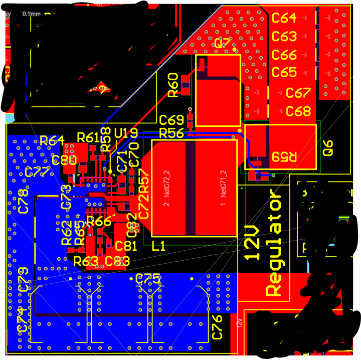 Bottom layer
 Schematic


