Other Parts Discussed in Thread: UCC28C56EVM-066,
Questions about UCC28C56EVM-066, (doc bumber sluucn1c)
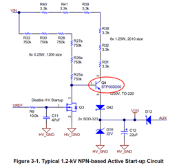
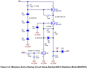
1. Q1, Q2 form HV startup for VDD, but zener D5 to Q2's gate, can not be breakup to generate a voltage of 25V. so what is the current path of D5?
2. Since voltage of VDD exceed 18V, VREFof UCC28C56H-Q1 powered up to be 5V, which trun on Q3, pull gate of Q2 to HV_GND, and finally turn off Q3.
HV Startup should be trun off, when AUX supply work normally. If Vref powered up to be 5V, before AUX supply work, HV startup was turned off, and take UCC28C56 into power down, and then power up.
This will not work probably.

3. Checking out BOM of this EVB, and I found some component can't be found on Schematic. U2, U3 for isolated feedback, can be found on BOM list, but there are no U2 or U3 on Schematic.
Where can i found complete Schematic?
4. What is the fuction of Leading Edge Blanking, and how can it work?