


Other Parts Discussed in Thread: TVS3301
Hi, I have a number of questions about using TPS26612 in the circuit below as depicted in the datasheet (page 31):
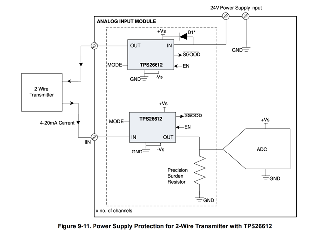
-
Is a TVS3301 recommended to be placed across the loop I/O pins AND/OR or between each pin and GND? This was specified in some of the other applications circuit diagrams for the TPS2661x, but omitted in this one. I would like some clarity on that choice.
-
In this arrangement, should both EN pins be toggled to disable the loop, or is just one of them acceptable? Are there any differences with using one over the other?
-
Which SGOOD should be polled? Are either okay? Is an OR necessary?
-
In short circuit fault-case where the TPS is current-limiting, are both ICs sharing the heat dissipation or will only one of the devices be limiting? If it will be a single device, which one?
-
Does +Vs have to be from the same 24V supply given that the overvoltage condition is (+Vs) + 1.50 [V]?
- Is the only purpose of the signal diode to prevent damage from the 24V input being wired in reverse, or is there a more intricate reason?
Thank you very much!
