This thread has been locked.

If you have a related question, please click the "Ask a related question" button in the top right corner. The newly created question will be automatically linked to this question.

TPS25750: TPS25750 Patch - PBMc not changing to APP

Part Number: TPS25750

Hi,

I am having some issues with the TPS25750. We have designed a prototype board with the TPS25750 as a feasibility study for USB-PD. In general use, the TPS25750 seems to work fine.

However, it gets into a certain state which I have difficulty getting it out of.

The state is as follows:

1) On startup, the boot-status register is read and DeadBattery bit is set and NoPatchConfiguration is set. (Note, I upload the configuration/patch over I2C)

Since the device indicates NoPatchConfiguration, I attempt to upload the patch over I2C. (This usually works fine, except in this case ...)

I follow the flow-chart (Execution flow Patch Burst Mode Example in the Host Interface Technical Reference Manual), and everything goes fine up until reading the result of the PBMc command.

So, having uploaded the configuration over I2C, I receive an ACK on the write transmission. Since the patch has been uploaded, I issue a PBMc command to the device, however, reading the data1 register results in a return code of 0x3, which I cannot make sense of from reading the manual... The rest of the output does not seem to indicate that anything has failed. However, upon completing PBMc with the result 0x3, I then wait for either patchloaded event or APP mode, and neither get set. So I am now stuck...

  • Hi Sven,

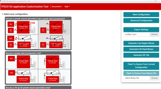
    Do you have a .pjt file that I may be able to look at in order to see what may be going on and to see what you are trying to flash? You can get this through the 'Save Project' under the 'Project' tab in the GUI. Are you saving your configuration as a full flash binary or low region binary? 

    Additionally if you can put the GUI into debug mode and take a snapshot after the device has been flashed this may be helpful as well, for this turn on debug mode under the 'Debug' tab in the GUI, then afterwards the Debug tab will have an option to take a snapshot.


    Could you try utilizing the 'DBfg' as well? Before or after. This can be found in section 3.4.1 on page 59 of the TRM linked here. Please let me know if or when you get the above information.

    Thanks,
    Field

  • Hi, 

    I will try and get the information you requested. I also have some Saleae traces of the problem if they are of interest. I run the DBfg task when I detect Dead Battery Flag on startup, and try and run the patch sequence after this. (Note: I am saving the configuration as low-region binary)

    Note, I don't use the Application Customization tool to flash, only an MCU.

  • I don't have the Project -> Save Project GUI options in my application. (Neither on the desktop app or in the online browser)

    I do however have a *.json config I could supply you with.

  • It wont let me upload the JSON file or the Saleae capture here, could I send them to you via e-mail?

  • Hi Sven,

    Saleae capture could be helpful! Are you supplying power to VIN_3V3? I believe .json should work fine. Normally you can drag and drop in here, but if that is not working please feel free to email them to me at f-tolson@ti.com

    Thanks,
    Field

  • config(1).zip

    This zip file should contain the relevant files.

    The “troubleshooting_pbmc_patch_issue.sal” I believe shows the entire sequence, from init of the device until a failed Pbmc.

    The “pbmc_after_successful_patch_transmit.sal” isolates the “problematic” Pbmc task with a failing error of 0x3.

     The config.json file is the configuration I am trying to flash.

  • Hi Sven,

    Thanks for this information.

    Maybe I am misunderstanding. You are trying to force dead battery and boot from it? Is this correct? And that it works normally outside of trying to force this/outside of this scenario?

    Thanks,
    Field

  • Not trying to force dead battery. At the moment it won't upload the patch no matter  what I do. Pbmc returns 0x3, and mode does not change.

  • Let me clarify: everything was working fine. I was doing some tests, like putting in sinks/sources, disconnecting batteries and so on, until O realized it was 'stuck' in 5V as sink. I looked into why, and saw the dead-battery flag in boot-status. I also saw there was NoConfiguration, so I attempted to reupload the patch. But I cannot upload anymore, for whatever reason. It is stuck in NoConfiguration mode with a patch sequence that 'fails' at Pbmc continuously.

  • Hi Sven,

    Okay. Thanks for the information! But I just wanted to make sure I understood. I believe this may be because it is booting in dead battery mode. Are you supplying a constant VIN_3V3 when attempting this? Do you have the capabilities to drive an unused GPIO pin high by chance? What is your ADC configuration (or the ADCIN decoded values)? Have you tried flashing it as a full flash binary instead of a low region?

    Thanks,
    Field

  • See the snippet from the schematic above regarding ADCIN configuration, there are jumpers to toggle between different settings. There is a constant VIN_3V3, which is shared with the interfacing MCU. I tried flashing a full flash binary, but there was no difference.

  • Just a quick question regarding the BOOT_STATUS register:

    Do I understand correctly that patchdownloaderr is bit 2 (0 index) on byte 1?

    The TRM states bit 10 is patchdownloaderr, but the reason I am asking is due to the fact that I sometimes see "information" on the reserved bits 4->9.

    As an example:

    I read BOOT_STATUS now, and get:

    [0x5,0x30,0x03,0xF0,0xC2,0xA1]

    0x30 is 00110000, which means bits 4 and 5 are set in byte 1, but the TRM indicates that these bits are reserved.

    0x03 is 00000011, which means bits 8 and 9 are set, (0 and 1 in byte 2), but the TRM indicates that these bits are reserved.

    Do the reserved bits mean anything? Is the TRM wrong? Am I misunderstanding?

  • Could any of the pins have an effect on the patching behaviour? If the PP5V is high for instance, could this have an effect?

  • Hi Sven,

    Reserved registers/bits/bytes can mean or indicate a myriad of things. Ranging from future use/design implementation to critical design features that shouldn't be changed. In this specific case, I do not believe it is for either of these, but I could be wrong. Since the TPS25750 is part of a family of devices similar to each other, the registers between devices can stay the same. If you look at the TRM linked here for the TPS65987, on page 37 it has register 0x2D the boot flag registers.

    • Bit 4 and 5, probably refer to Region0 and Region1 which indicates the specific region of the SPI memory was attempted.
    • Bit 8 and 9, probably refer to Region0FlashErr and Region1FlashErr, which indicates that an error occurred attempting to read the specific region of SPI memory. 

    But to me this makes sense since you are unable to upload the patch/flash to the device. It's possible that the pins could have an effect, but if you are supplying VIN_3V3 then the device should respond properly. You will want to make sure VBUS is present at the PD controller as well.

    Could you try utilizing the 'Gaid' or 'GAID' commands and seeing if either allow you to restart or able to upload thereafter? This can be seen in the TRM that I linked earlier on page 112 and 113 accordingly. Another option may be to utilize the GPIO event 'barrel_jack_event', if you can drive a GPIO pin high that may clear this dead battery flag. DBfg command is also a route, but you said that wasn't working correct? 

    Thanks,
    Field

  • OK, fair enough. It's slightly misleading though that I would have to look in the TRM for another part to "sort of" make sense of the bits for a register in a different part...

    I tried GAID with no success on a previous occasion (there was no reference of GAID in the TRM for TPS25750, I 'found' it by browsing the forum..).

    I managed to get it out of the strange state, without knowing exactly what I did, but this issue is not resolved. I want the root cause identified, and how to get out of it.

    To summarize the cause of my problem in one sentence:

    * What should we do if the device can not be patched over I2C externally, if Pbmc fails?

    Steps are as follows:

    1) Patch flow OK, up until issuing Pbmc command. The command is accepted (no !CMD), but reading data1 register shows 0x3 as the first byte.

    2) 0x3 as a return code from Pbmc is not documented well (at all?) in the TRM, which it should be as it seemed to really mess me up.

    3) Apart from Pbmc returning 0x3, this causes the device to not switch from PTCH mode, and the PatchLoaded event is never set.

    Please help me determine what could cause the symptoms reported above, and how to get out of it.

    (Note : What seemed to help me in the end was turning off PP5V before attempting the patch, however, I cannot confirm this and I believe it went OK before when PP5V was high.)

    This is an evaluation to see if TPS25750 is going to suit our purpose. If this issue is not resolved,  I am not sure whether we will go for TPS25750 in the end.

  • Hi Sven,

    I understand, agree, and don't know why it is not listed in the TRM for the TPS25750. 

    As mentioned I believe this had to deal with dead battery mode. Which usually occurs when VIN_3V3 is no longer powered and switches to VBUS until this is resolved. Once this is resolved, then normally you should be able to clear the dead battery flag using the DBfg command and resume the normal procedure. Because these commands did not work, I wonder if the device was constantly using the VBUS instead of the VIN_3V3, as you said you were supplying VIN_3V3, and thus the device would still be in a perpetual dead battery. In which disconnecting PP5V may have worked. If this is the case or the problem, I do not know and how you got to the beginning point to begin with, I do not know either.

    I understand. I am going to take another look at your configuration again to see if there may be something I missed, as well as try to see if I can replicate behavior/issue on the EVM with power requirements being met. I will also try to discuss this with another expert in hopes of getting to the bottom of this but may require more time. 

    Thanks,
    Field

  • Thanks for your understanding. Slight smile

    I can trigger the state quite regularly now, and I still find it hard to get out of.

  • Hi Sven,

    Since you are able to do this regularly may I ask what you are doing to get into this state/trigger this? Does removing PP5V solve this issue? 

    Thanks,
    Field

  • No, removing PP5V does not resolve the issue. By removing the batteries, and only having a source (power supply) connected to the TPS25750. That is what I do to trigger the state. (Or so I suspect)

  • For context, here is an output of my state-machine for the patch flow:

    0> 101-TPS25750::[INIT]
    00> 103-TPS25750::[STATE_CHANGE] 0 -> 2
    00> 204 :: TPS2570 :: [PATCH_RDY] = 1,2 /* Wait for patch ready event or mode */
    00> 205-TPS25750::[STATE_CHANGE] 2 -> 3
    00> 302 - TPS25750 :: Patch download starting! /* Write patch-info to data1 */
    00> 303-TPS25750::[STATE_CHANGE] 3 -> 4
    00> 408 :: TPS2570 :: [CMD] PBMs = 0x0 /* PBMs succeeded with 0x0 */
    00> 408-TPS25750::[STATE_CHANGE] 4 -> 5
    00> 6125 - TPS25750 :: Patch download complete! /* Patch/config written down with ack */
    00> 6125-TPS25750::[STATE_CHANGE] 5 -> 6
    00> 6202-TPS25750::[STATE_CHANGE] 6 -> 4
    00> 6308 :: TPS2570 :: [CMD] PBMc = 0x3 /* PBMc failed with 0x3 */
    00> 6308-TPS25750::[STATE_CHANGE] 4 -> 7
    00> 6308-TPS25750::[STATE_CHANGE] 7 -> 9
    00> 6703-TPS25750::[STATE_CHANGE] 9 -> 7
    00> 6802-TPS25750::[STATE_CHANGE] 7 -> 4
    00> 6920 :: TPS2570 :: [CMD] PBMe = 0x3 /* PBMe failed with 0x3 */
    00> 6921-TPS25750::[STATE_CHANGE] 4 -> 7
    00> 7002-TPS25750::[STATE_CHANGE] 7 -> 4
    00> 7108 :: TPS2570 :: [CMD] PBMe = 0x3
    00> 7108-TPS25750::[STATE_CHANGE] 4 -> 7
    00> 7202-TPS25750::[STATE_CHANGE] 7 -> 4
    00> 7308 :: TPS2570 :: [CMD] PBMe = 0x3
    00> 7308-TPS25750::[STATE_CHANGE] 4 -> 7

    00> 7401-TPS25750::Too many retries, attempting recovery
    00> 7402-TPS25750::[STATE_CHANGE] 7 -> 14
    00> 7402-TPS25750::[RECOVER]
    00> 7403-TPS25750::[STATE_CHANGE] 14 -> 4
    00> 7508 :: TPS2570 :: [CMD] Gaid = 0x0 /* Gaid succeeded, wait 500 ms */
    00> 7508 - TPS25750 :: GAID delay
    00> 8103-TPS25750::[STATE_CHANGE] 1 -> 0
    00> 8201-TPS25750::[INIT]
    00> 8203-TPS25750::[STATE_CHANGE] 0 -> 2
    00> 8317 :: TPS2570 :: [PATCH_RDY] = 1,2 /* Wait for patch ready event or mode */

  • Hi Sven,

    Thanks for the information. I have not been able to recreate this and I am still looking further into it and apologize for any delay. Could you tell me which pins are supplied by your ''source (power supply)'' that you described above?

    Thanks,
    Field

  • Hi,

    I sent you some data via mail. Here is a snippet from the raw I2C buffer after the PBMc command fails:

    I read 40 bytes. There is some data there, is there anything you can gleam from it regarding cause of error?

  • Hi Sven,

    I received and replied to your email. I am still currently working on this.

    Thanks,
    Field

  • Hi, any news here? I tried changing the TPS25750 device with another one, as I suspected ESD, but the problem persists on the new device. There must be something in the data that could explain why it won't apply the patch??

  • I have the same problem:  after sending PBMc to the CMD1 and reading DAT1 register I get 0x03 in the first byte. The MODE register is still on PTCH, while it should switch to APP. Please help.

  • Hi,

    Field is currently out of office. He will be back next week.

    Regards

  • I noticed that the ReadyForPatch flag in the INT1_EVENT register is 0, also after looping with 10ms delay.

    According to  the patch execution flow this should be set (1)?

  • Hi Sven,

    Apologies for the delay as I have been out of the office. Based on the .sal's that you sent me, it looks like you may be writing/reading to and from the wrong device sometimes. There may be a bit shift that you are implementing or experiencing, which may be some explanation for the weird data you are receiving and commands not working.

    For example, here and in other you are writing/reading/accessing to 0x10. Could you try changing these to the 0x20 address? And verify the other information you are trying to send to the device is not additionally/possibly experiencing this.

    The 0x3 you are reading or have read before, I believe this is for 'failure', either due to incomplete data, or incorrect data sizes. Which may have to deal with the above information.

    @ Jan, you may want to check for something similar to the above and ensure you are using the correct address. Which may or may not remedy the issue.

    Thanks,
    Field

  • Hi Field,

    Thank you for your reply. There did seem to be an issue with the patch-mode address. By explicitly using 0x10 as the patch address, writing the patch seems to work and Pbmc returns 0x0. However, I have to write the whole patch at once. If I try to do a partial write (write in chunks until the whole patch is transferred), I only get up to 1024 bytes or so before the "write" operations start failing with NACK. Is there any updated documentation which describes the patch flow in sufficient detail?

  • I did some experiments with changing the bundle size in DATAx.  The bundle size that can be written before NACK is received varies with this, but not as would be expected.

    What would be the correct way to specify a 32k bytes bundle size?

    bundle size = 0x7D00

    According various sources, the I2C packet for preparing the transfer should look like (hex values):   

    09 06 00 7D 00 00 50 32

    where 09 is for addressing the DATA1 register, 06 is for  the number of bytes to be send, 00  byte 1 of the bundle size, 7D byte 2 of the bundle size, 50 the I2C address to transfer the bundle and 32 the timeout. But this does not work, it gives an NACK after transferring 31744 bytes, as if the bundle size would be 0x7C00.  Encoding 7E instead gives NACK after 31872 bytes, as if bundle size would be 0x7c80.

    I transfer the bundle in chunks of 64 bytes.

    When I transfer in chunks of 128 bytes instead, I get better results, namely all 32k bytes are acknowledged, but I still get back 

    40 03 00 00 00 51 32 00 .....  when I read the DATA register after PBMc and the MODE stays in PTCH.

    The BOOT_STATUS reads 30 03 60 02 a1 which would indicate that  "No configuration has been loaded"

  • Hi Sven,

    There is the patch flow process in the TRM on page 62 linked here, but I think this is the one you may already be looking at or following and I will see if I can find something in more detail. 

    @ Jan, can you create a new E2E and reference this one as your issue may, or may not, deal with something different, and will allow us to help you better accordingly. In this new thread it would be helpful if you include your information from here, as well as any Saleae captures you have, and .pjt file or .json file from your configuration. Aside from that, similar to the current discussion you may want to check the address you are writing/reading/acknowledging from.

    Thanks,
    Field

  • Hi,

    There is still an issue! I tried doing a patch on every startup, just to gauge the stability of the device. If PBMc gets into the 'funny' state where it returns 0x3, it is very hard to get out of....

    I don't know what to do at this point.

  • Hi Sven,

    Is this happening each time or only on select occasions? If select occasions is it possible for you to collect the data from one of the scenarios where it works and one from where it doesn't? Are you patching the same information each time or changing the information with each iteration? And what are you doing to get out of the state, does re-patching not work here? 

    Thanks,
    Field

  • pbms_capture.zipHi,

    On select occasions, but I still do not know the root cause. It has something to do with loss of power, when the TPS25750 loses it's configuration. It is the same information that is being patched each time, this does not change.

    The code does not change either, but sometimes the device does not respond as it usually does.

    Not sure how I get out of it either, it seems to just "resolve" itself from time to time....

    As of right now, it is in a state I have not seen before. The PBMs command times out (the empty command string is never received) when trying to patch.

    I have attached the Saleae capture of the relevant scenario. (Both CSV and Logic 2 *.sal file)

  • Hi Sven,

    Thanks for providing these. Are you trying to utilize the 'GAID" command in these? It looks like some times G A I or G A (something else) D, etc are populating but not finishing out and I am not sure. Would you be able to or would utilizing EEPROM instead of MCU be viable? 

    Are you losing power during these transactions?

    Can you look at the Execution Flow diagram on page 53 of the technical reference manual linked here, and follow it step by step (and I assume you already are), and let me know when and where you are experiencing the problem or how far you make it? And the problem that you are seeing? As you said PBMs is timing out but you also mentioned PBMc is in a funny state as well. The problem must be before these steps where the error occurs (assuming VIN_3V3 is high). I just do not know where. Are you utilizing the PBMe command as well?

    Thanks,
    Field

  • Hi,

    Yes, I perform GAID as a recover step when something times out.

    I am following the Execution Flow, however, I did find a point where I was not following fully.

    When waiting for "Patch Ready", I am waiting for PatchReadyEvent or Device Mode PTCH.

    This should be an AND according to the execution flow. When changing the logic so that both conditions have to be fulfilled before starting the patch process, I see that the PatchReadyEvent never goes high.

    This could perhaps explain why PBMs is timing-out right, as the device is not strictly ready for a patch even if it is in patch mode? Is there any reason why PatchReady event does not go high?

    I am looking into using an EEPROM, but there seems to be very little information avaiable online as to how one would go about doing this:

    * Any specific type of EEPROM?

    * Which address should the patch be written to?

    * Any header information?

    So, I suppose I require the following pieces of information:

    * Why does PatchReadyEvent not go high?

    * More information about how to configure an EEPROM with the patch information (see questions above)

  • Hi Sven,

    I am not in the office today and will look into this and provide a response tomorrow when I return.

    Thanks,
    Field

  • Hi Sven,

    Why does PatchReadyEvent not go high?

    I am not entirely sure. Based on your most recent Saleae capture, it looks like to start the patching process that you are reading from 0x16, could you try reading from 0x14 and sharing the transaction? There's also something different here, as there should be 11 bytes returned for the byte count, but it looks like the device is returning 5. But this may have something to do with looking at 0x16 first before the patch, but maybe not. I'm still trying to dive into why this PatchReadyEvent wouldn't go high if power is supplied. Are the I2Cs_SDA/SCL lines pulled up through a resistor? Assuming this is where the data is coming from, and where you are testing is from. Is there any data on the I2Cm_SDA/SCL lines when this is seen as well?

    In regards to the EEPROM, for the TI reference design for the TPS25750 it looks like the CAT24C256WI-G, datasheet linked here, is being used as the EEPROM for the device. You can see this in section 2.4.1 on page 6 of the reference design linked here. Based on this reference design it looks like the CAT24 address pins are set using 10kΩ resistors to ground corresponding to the next statement for the address to meet the address requirement. Which the datasheet for the TPS25750 states that the external EEPROM shall be at 7-bit slave address 0x50, this can be seen in section 9.4.1 on page 45 of the datasheet linked here. It should be different in that you can just flash the binary file to the EEPROM from the GUI and the device then reads and processes the rest as the master device to the EEPROM device, and not have to go through this whole patch process. 

    Thanks,
    Field

  • Hi,

    Not sure about the 0x16 thing, I will look into it next week.

    However, I will not be using the GUI to flash the EEPROM, I will flash it from an MCU.

    Thus, I need to know where the configuration binary should be flashed to on the EEPROM so that the TPS25750 will "find it".

    Let me rephrase it:

    The TPS25750 "checks" that there is an EEPROM on address 0x50 on it's master I2C bus, if there is, it will download the configuration that it finds on there. Which address on the EEPROM does it expect to find the configuration, and how does it know how large it is? I would expect there to be a header at a fixed memory location (0x0 for instance) on the EEPROM of the sort:

    typedef struct TPS25750_hdr {

    uint32_t cfg_offset;

    uint32_t cfg_size;

    };

    Which holds information about where the configuration is stored, and how large it is. Please explain how to program the EEPROM so that the TPS25750 will find and download the configuration directly.

  • Hi Sven,

    Please allow me a little bit more time to dig through more files for you to see if I can find this specific information as I wasn't immediately able to find it.

    Thanks,
    Field

  • OK, thank you. Some additional information though:

    1) PBMs is consistently timing out if I do not wait for PatchReady event.

    2) If I wait for PatchReadyEvent, it never goes high.

    3) However, the GPIO status seems to be updated correctly. (One of the GPIO status pins is 1 (UFP event))

    I updated the configuration to control some of the GPIOs based upon events. There are three events I am interested in (cable orientation, UFP/DFP and plug-present). As stated previously, the UFP/DFP GPIO is updated correctly based on the status, so this seems to suggest that the application is partly running? But the boot-status states that no configuration is loaded.

    As I said, I am working on getting a new prototype board built with an external EEPROM. Still waiting on information how to program the EEPROM from an MCU.

  • Hi Sven,

    Were you able to check from 0x14? But I suppose even if it was high and we were looking wrong, it would be irrelevant because you are still trying PBMs. The problem is, based on your most recent Saleae captures, is that when you are trying to read from register 0x16 it is returning 5 bytes, but I believe we are expecting 11 and am hoping that 0x14 would return this.

    • Does the device sink or source corresponding to the PDO's that you have set through this patch or information?
    • Are you power cycling the device each time?
    • Before uploading the patch, what does register 0x03 return, does it return 'PTCH'? 
    • After the first instance of PBMs, what does register 0x08 return, does it return '!CMD'? 
    • In your most recent Saleae capture. It looks like some interesting things are happening:
      • After reading from 0x16, which I assume is where you are trying to check for ReadyForPatch, you then try to write to register 0x01, which should not be written to.
      • You try to use the following registers:
        • 0x0A
        • 0x02
        • 0x04
      • You try to use the following addresses:
        • 0x40 address, for the register 0x06
        • 0x24 address
        • 0x00 address
        • 0x40 address, for the register 0x02
        • 0x39
      • You try writing to 0x08 as the command register but you send the command ' (!&9 ', but you also gave this a byte count of 2. It looks like the incorrect byte count was given a couple of times for your write commands. 
      • It also appears a couple times that you are trying to force read PBMs and not write. 
      • I do not recall you utilizing register 0x09 before the PBMs either.

    It looks like the above happen multiple times as well as others. But I could be reading or interpreting these wrong, as you say it works sometimes. I am going to meet with another expert tomorrow to verify or look more into it. 

    In regards to the EEPROM: using the reference design mentioned above, (from my understanding) you would use this CAT devices address and using the SDA/SCL, you would then write the entire binary file that you developed from your project/configuration to this device. It may help to have 0Ω resistors to able to disconnect the MCU from the EEPROM and points to be able to attempt to flash it manually. 

    I hope to have an update by EOB tomorrow regarding the above register/address information.

    Thanks,
    Field

  • PBMs_Timeout.zipHi,

    Not sure what you are talking about at all regarding the capture... I think you were perhaps being confused by other devices on the bus.

    I made a new capture, where I isolated the traffic to the TPS25750, showing the PBMs timeout in detail.

    When the capture starts, I have already verified that the mode is in patch.

    Steps (from the capture):

    1) Start writing 0x9 register

    2) Write to 0x8 register (PBMs)

    3) Read 0x8 register waiting for command complete.

    As you can see, PBMs remains in 0x8 until timeout.

    So, this is what I am experiencing right now....

    Note, the mode is in patch, but the PatchReady event is not set. (The entire event register is 0)

  • I replaced the TPS25750, and things improved. Perhaps the TPS25750 was "damaged" in some sense, so no need to look into this. I think we can resolve this case as soon as I receive the details on how to program the EEPROM. Slight smile

  • Hi Sven,

    That is good to hear that it is now improved. And I do think that is where my confusion is from.

    Regarding the EEPROM, if your design is now working as intended then there may be no need for it? It was a suggestion to try and work around your current issue as our EVM's use EEPROM. But to dive deeper into it there are a couple of resources: 

    • Linked here is an application report that covers the programming of EEPROM via I2C using an MSP430. This covers the byte write and page write commands
    • Here is the datasheet for the EEPROM device we/I was discussing earlier and can be seen in the reference design also mentioned earlier. This covers the page write and byte write timing. Please note that this is not a TI device so I can not speak for it.

    Both of these cover the bytes, bits, address, and data being sent and how they should be used correspondingly. Upon powering up the PD device looks to the EEPROM for the configuration correspondingly and loads it, all that needs to happen is have the data loaded to the EEPROM using the above information/reports/sheets.

    Thanks,
    Field