Hi team,
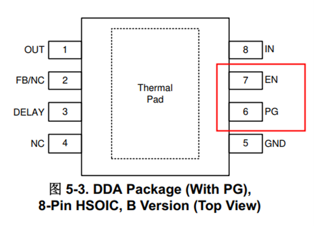
1、Is there a more detailed schematic design reference diagram for the EN and PG pins?

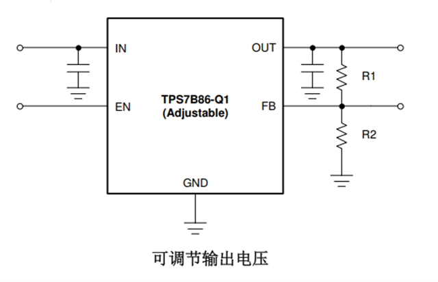
2、When the TPS7B86-Q1 application circuit design output is 12V, are there any specific recommended values for the R1 and R2 resistance values of the FB pin?


