


Hi, my goal is to design a buck circuit with TPS62933. Input=24VDC, Output=10V 3A.
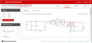
Design: Use Wenech to design the circuit
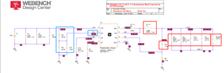
Simulation: Use Pspice for TI + TPS62933 PSpice Transient Model to validate the above circuit. According to the webench design, I did the following modifications to the example PSpice circuit (see red box). The simulation result is given below.
Questions
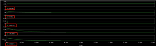
1) Why V(SW) is graduallt decreasing? It should be a 0 or 24V switching signals. As a result, I(RLOAD) and V(VOUT) are NOT 10V 3A.
2) See blue box, why 24V with two 49.9kOhm voltage divider makes EN pin = 5V? It should be 12V by resistor votlage divider.
3) At the output load, why the simulation result decreeases to 0V, but label still shows 5V?
Thank you very much
