This thread has been locked.

If you have a related question, please click the "Ask a related question" button in the top right corner. The newly created question will be automatically linked to this question.

BQ24296MEVM: Some question and shematic review

Part Number: BQ24296MEVM
Other Parts Discussed in Thread: BQ24296M

Hi,

I have some questions and schematic review demand as below.

1.How long does it take for the Shipping mode to be entered after setting REG07[5] to 1 (BATFET_DISABLE) via I2C?

2.When the input current limit is set to 1A, PSEL is connected to GND, and OTG is left unconnected?

3.Can the QON pin be left unconnected when not using a physical button to exit Shipping mode?

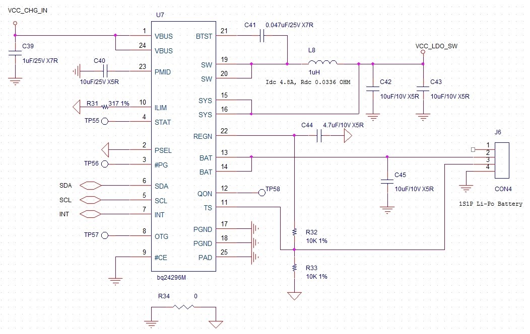
4.Please assist in verifying if the following circuit has any errors.
  • Hi Jeff, 

    Please see my comments below. 

    1) It will take approximately 60usec from the end of the I2C communication to REG07[5] for the device to enter shipping mode. Waveform included below shows the timing of the I2C write compared to when Vsys drops due to entering shipping mode. 

    2) Referring to table 2 from BQ24296M datasheet connecting PSEL to GND will set input current limit to 3A. The actual input current limit will then be further reduced due to the resistor setting at ILIM. Your current schematic design will limit input current to typical ~1.37A. The IINLIM register setting in REG00 can be set to 100b to set input current limit to 1A. 

    Based on table 2 when PSEL is high the state of OTG pin will have no effect on the input current limit, but OTG pin should not be left unconnected. Depending on if you plan to use the boost mode feature the OTG pin either needs to be driven high or connected to GND. 

    3) Yes QON pin can be left unconnected. 

    4) Schematic review feedback:

    -OTG pin should not be left unconnected. It needs to be driven either high or to GND depending on if you plan to use boost mode in your application. If you have no intention to use boost mode then connect OTG to GND. 

    -Please ensure SDA and SCL lines are connected to a logic rail via a pull up resistor.

    -Connecting TS pin between two 10kohm resistors is correct if you do not plan to use a NTC thermistor. In the schematic there is a connection from TS to the battery pack pin 3, which appears to be the connection to a pack thermistor. If this is the case R32 and R33 need to be resized according to the equations on page 23. 

    The rest of the schematic looks okay. 

    Best Regards,

    Garrett 

  • Hi Garrett,

    Thanks for respones. There stil some qeustion as below.

    1. What is the relationship between PSEL, ILIM pin, and register REG00? In case of conflicts (e.g., ILIM pin resistor value set to 1A and REG00 configured to 110 for 2A), which setting takes precedence?

    2. In the calculation formulas for RT1 and RT2, are Vltf and Vtco 73.5% (Typ) and 44.7% (Typ), respectively, as a percentage of VREGN 5V (3.675V & 2.235V)?

    3. Should RT1 and RT2 be determined based on the NTC specifications used in the battery and the temperature range for battery charging to set RTHcold and RTHhot?

    Thanks!

    Jeff

  • Hi Jeff, 

    1) The actual input current limit will be the lower value between ILIM pin and REG00 setting. For the example you gave ILIM pin takes precedent. Similarly if ILIM pin sets current limit to higher value than REG00 setting then register setting takes precedent. The state of PSEL when input adapter is plugged in causes REG00 to be updated as described in datasheet section 8.3.1.3.3 on page 17. 

    2) Yes V_LTF is 73.5% and V_TCO is 44.7% as a percentage of VREGN since REGN is the pullup rail for TS resistor divider network. 

    3)Correct, RT1 and RT2 should be calculated based of the NTC resistance at the desired temperature range you wish to charge at. The example provided in the datasheet where RT1 = 5.25 kohm and RT2 = 31.23 kohms corresponds to setting charge temperature range from 0°C to 45°C and using a 103AT NTC thermistor. 

    Best Regards,

    Garrett