This thread has been locked.

If you have a related question, please click the "Ask a related question" button in the top right corner. The newly created question will be automatically linked to this question.

TPS7A57: Simulation error after 1.2V output.

Part Number: TPS7A57
Other Parts Discussed in Thread: DAC63204

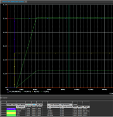
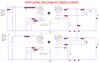
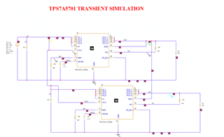
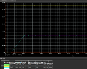
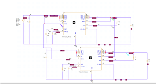
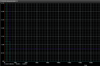
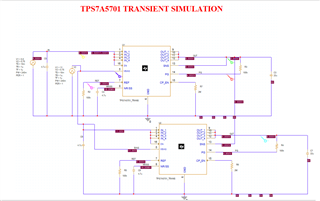
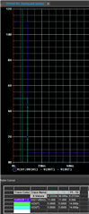
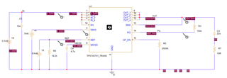
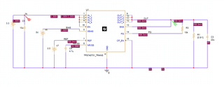
According to feedback resistor, we set the output voltage but in simulation (PSpice) we notice that if the output voltage exceeds the 1.2v, the simulation stuck and gives the error. It looks like the output move than 1.2V is not supported. Can you check and confirm why this is happening?

Mohsin

  • Hi Mohsin, 

    Thank you for reaching out and sharing this with us. 

    Can you please share your circuit with us? The model was tested to simulate up to Vout=5.2V. Notice the results for 1.2V

    Please make sure that the necessary changes are made, i.e correct Vin levels, correct Vbias, correct Iout values. 

    Best, 

    Edgar Acosta

  • Hi Edgar

    Please find the SS of the circuit below.

    Regards

    Mohsin

  • Hi Moshin, 

    I ran the simulation as following: 

    I am getting 1.2V on the output

    Even when I run it as following: 

    I have replicated the exact same circuit you provided and I still get 1.2V. 

    Can you share with me your simulations settings and the options section? 

    Best, 

    Edgar Acosta

  • Hi Edgar

    I am also getting 1.2V but not more than 1.2V. If the resistor feedback change to more than 1.2V output. The simulation stops and gives the error. Can you check on your side whether this is the same or not?

    Regards
    Mohsin

  • Hi Edgar

    The above schematic share by you is not even working for me. Can you guide me about the simulation settings and options section? What you are trying to explain?

    Thanks
    Mohsin

  • Hi Mohsin, 

    I'll try simulating by changing the Ref resistors to higher Vouts, however the circuit configuration is somewhat odd and doesn't seem to be a common use case. 

    May I ask what is the intention? Are you trying to parallel the LDOs? Or what is the purpose of tying the SNS of one LDO to the the output of the other? 

    By looking at each individual LDO, one should provide a Vout of 1.8V and the other 0.9V. It could be that  by connecting the LDOs in such manner, PSpice can break since it is not intended to be connected that way. 

    Best, 

    Edgar Acosta

  • Hi Mohsin, 

    Quick update. I changed Vout to be equal 5V on each LDO: 

    And still no issues. 

    Are you providing the correct Bias level for higher Vouts? 

    Again, can you share more information of why the circuit is connected in such a way? Also, can you share your options from your simulation settings? 

    Best, 

    Edgar Acosta

  • Hi Edgar

    I just downloaded again the fresh simulation files from TI and run the simulation. Same issue is coming and the see the SS for the simulation settings option below:

    I can't understand what is happening wrong here.

    Regards
    Mohsin

  • Hi Mohsin, 

    These are the same settings I have on my end. 

    Have you tried running a single device by itself? 

    May I ask what is the intention? Are you trying to parallel the LDOs? Or what is the purpose of tying the SNS of one LDO to the the output of the other? 

    Again, if the intention is to parallel the LDOs, the configuration is different. 

    I would also highly suggest looking at : TPS7A57EVM-081 Evaluation board | TI.com

    and reading through: Scalable, High-Current, Low-Noise Parallel LDO Reference Design (ti.com)

    TIDA-050061 reference design | TI.com

    Comprehensive Analysis and Universal Equations for Parallel LDO's Using Ballast

    Parallel LDO Architecture Design Using Ballast Resistors (ti.com)

    Best, 

    Edgar Acosta

  • Hi Edgar

    I tried to use single IC and its simulation doesn't work more than 1.2V output. The same case I am facing with 2 IC's. The problem is that why I am not getting the output more than 1.2V, even with single chip?

    Regards
    Mohsin

  • Hi Mohsin, 

    What is the Rref value you are using for higher Vouts? I recommend trying with two different sources for Vin and Vbias. 

    Make sure that Vbias is set properly. This device has the following table listed in the Data Sheet: 

    It is recommended to set Vbias at least 3.2V higher than Vout, therefore, Vbias=Vout+3.2. 

    The model was set to function as close as possible to Table 7-1. If there is no Charge Pump voltage, then Vbias has to be higher than 3V. 

    The model also checks if BIAS is higher than Vout+2.1V, but it recommended to use a higher value than 2.1V. 

    Best, 

    Edgar Acosta

  • Hi Edgar

    I tried to change the VBais to 5V and it doesn't work but If I increase it to 8v or more then it starts working for like 0.9v output. Can you explain why it is not excepting it at 5V?

    Regards
    Mohsin

  • Hi Mohsin, 

    Can you share your new schematic in addition to the errors and/or output waveforms? Also, can I see your auto converge settings? 

    Best, 

    Edgar Acosta

  • Hi Edgar

    Please find the SS for the schematic, Output errors and auto converge settings.

    Regards
    Mohsin

  • Hi Mohsin, 

    Can you remove the 0.5V source at the REF pin? This is overriding the REF to 0.5V, therefore your output becomes 0.5V as well as this device is intended to work in unity gain. 

    Best, 

    Edgar Acosta

  • Hi Edgar

    It is working without 0.5V source already. But we need this source in our design. as this is acting as a reference external source from other than the feedback resistor. as I mention earlier, If I change the VBIAS to 8V, the circuit works.

    Regards
    Mohsin

  • Hi Mohsin, 

    Is it possible to know why the device needs an external source for the reference? What type of reference is it being added? 

    I have removed the Rref and placed a 0.5V reference and it works with a Vbias rail of 5V: 

    Best, 

    Edgar Acosta

  • Hi Edgar

    We are using external source for changing the feedback using controller and setting deferent outputs. Also we need Rref as well for initial start. But tell me which software version you are using because the circuit you SS above is not working in my simulation.

    Regards
    Mohsin

  • Hi Mohsin, 

    Is this external source a DAC? Just be aware that depending on the source, you can possibly inject noise into the REF node. 

    This is the current version I'm using: 

    I highly recommend using an EVM for this sort of evaluation. This LDO has several ABM blocks internally in addition to some R and C that help the model converge. Putting an external voltage on the REF can impact the behavior of the model and PSPICE might not be able to converge properly. 

    Best,

    Edgar Acosta

  • Hi Edgar

    YES, I am using a good low noise External DAC source. 

    Our simulation is working without the DAC source but once I will add the source the simulation doesn't work. Is this a simulation software issue of the chip or the chip can't handle this external DAC in real?

    Regards
    Mohsin

  • Hi Mohsin, 

    Thank you for the information. 

    This is simulation related. The device can perfectly use a DAC. Section 8.1.16 and 8.1.17 in the data sheet talk about using DACs for voltage margining: 

    Best, 

    Edgar Acosta

  • Hi Edgar,

    The sections in the datasheet you refer to above only work with a DAC that can sink and source current. Both the current margining the voltage margining mode. In this case, the DAC is only used to set the reference voltage. The application is different, the DAC is not used to margin but to set the reference voltage.

    Thanks,

    Arnav

  • Hi Arnav, 

    I agree, the sections show margining, however, the same concept can still be applied with just a voltage DAC. We have seen applications where the voltage DAC is straightly connected to the REF without sinking/sourcing current. 

    I guess my question would be, what is the application for using this external reference, and/or why is an external reference needed if there is no margining.  

    I highly recommend evaluating this at bench using an EVM. 

    Best, 

    Edgar Acosta

  • Hi Edgar,

    Using the Rref is a nice to have to set the nominal output of the LDO before the DAC EEPROM is programmed. The DAC POR value will be pull high at 3.3V setting the reference too high. We have a jumper to disconnect the DAC connection, but I don't want the Rref pin to be left floating. 

    We have a design with the TPS7A57 but without the resistor, I will try to solder it and test. 

    Thanks,

    Arnav

  • Also we do still margin the voltage by simply change the DAC code/ voltage level. Its much more straight forward that finding a DAC that can source/sink current and calculating the current to support margining that way. I think that application in the data sheet is too convoluted and limited only allowing you to margin a certain percentage. Using the DAC directly to set the reference will allow more direct control. 

  • Hi Arnav, 

    Thank you for the information. 

    Yes, having a resistor is ideal. Specially if the LDO will be ON before the DAC. During steady state, there shouldn't be any issues, but there is an internal switch between NR/SS and REF, this switch closes depending on the condition for Vref, therefore, to prevent any undesired/abnormal behavior, it is recommended to have Rref installed. 

    3.3V at the reference is still ok from the LDO perspective since the recommended max 5.3V.

    As far as the application discussed in data sheet, it is an example to showcase that margining is doable and depending on the application the % can vary.

    Due to the internal current source to set Vref and knowing that Voltage Margining and Scaling is a primary application for the DAC63204, a current DAC + sink/source capabilities was chosen and preferred as it was easier and convenient to just change the code to change the current.

    Best, 

    Edgar Acosta