This thread has been locked.

If you have a related question, please click the "Ask a related question" button in the top right corner. The newly created question will be automatically linked to this question.

BQ24296M: EMI issue during PMIC switching

Part Number: BQ24296M

Hi.

Our prototype design with BQ24296M has an EMI issue. Could you look at the design? Maybe there is something I'm missing.

Issue description:

  1. The design shows vast RF noise floor degradation (up to 10 dB @ 868 MHz) when supplied from the +VPSU.
  2. The noise floor degradation correlates with the applied +VSYS load (more current - more noise). There is no noise with a light load (<300 mA)
  3. The amount of noise doesn't change while replacing the +VPSU source.
  4. Replacing the inductor with a fully shielded one or adding the ferrite bead at +VPSU doesn't affect the noise.
  5. Replacing the VBUS decoupling capacitor with 1 uF makes the noise worse.

Additional information regarding this system:

  1. IINLIM 2.0 A
  2. VSYSMIN 3.5 V
  3. ICHG 640 mA
  4. Average system current w/o charging - 250-300 mA
  5. Peak system current w/o charging ~3.5 A (short GSM bursts)
  6. The 868 MHz transceiver has a 32 MHz crystal, so it may be sensitive to the noise harmonics on 64 MHz, 96 MHz, 128 MHz, etc.
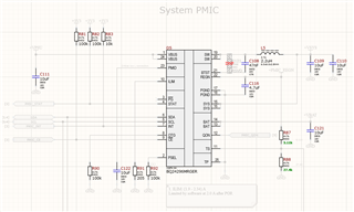
The schematic:

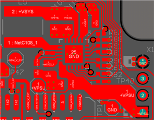
The layout (4L PCB, SIG+PWR - GND - GND+PWR - SIG+GND):

  • Hello, 

    Please see my recommendations below. 

    First I have a few recommendations for EMI suppression components you can look to add to your schematic to help reduce EMI. 

    1) Add a 1 nF capacitor at PMID, SYS, VBUS (optional), and BAT (optional). The purpose is to add this high frequency cap which works in 100MHz to 200MHz range to return high frequency noise to GND. 

    2)Add resistor (in range of 0 ohm to 10 ohm) in series with BTST capacitor from BTST pin to SW pin. The purpose is to reduce the switching slew rate. We do not recommend using higher resistors values than 10 ohm as it will start to adversely affect converter efficiency.

    3)Add a snubber circuit (resistor and capacitor) from SW pin to GND. Use R = 1ohm and C = 15 nF as reference, but TI recommends to try several different combinations to get best results with your custom PCB design. 

    Regarding your layout I do not see any obvious issues, but I have a couple suggestions. You already have the input capacitors, REGN capacitor, and BTST capacitor all placed close to the IC as recommended.

    -One recommendation is to add a few additional vias to your thermal pad. TI recommends to use a 3 by 3 grid (i.e. 9) vias for the thermal pad. Your design currently only uses 5.

    -We also recommend you directly connect the GND trace at PGND pins 17 and 18 to the thermal pad on the top layer. 

    Best Regards,

    Garrett 

  • Hi Garrett, and thank you for the suggestions. I will run them and leave a comment here. Slight smile

    Regarding the series resistor for the bootstrap capacitor - do you have any ready-to-use guidelines on how to check its power dissipation (except physical verification)? This design is dense, so I'd like to stick with 0402, which can't hold too much heat.

  • Hi Vasyl, 

    I do not have any guidelines for how to check its power dissipation. I checked what we have done in the past with our evaluation board builds and we have used a 0402 resistor in the past for BTST resistor (as an example BQ25890EVM uses a 0402 resistor at BTST pin). Therefore it should be okay, but I would still recommend performing verification on your unique PCB design. 

    Best Regards,

    Garrett