Because of the holidays, TI E2E™ design support forum responses will be delayed from Dec. 25 through Jan. 2. Thank you for your patience.

This thread has been locked.

If you have a related question, please click the "Ask a related question" button in the top right corner. The newly created question will be automatically linked to this question.

TPS650864: TPS6508640

Part Number: TPS650864
Other Parts Discussed in Thread: TPS650860EVM-116

I made a design with your product part number TPS6508640. When the system voltage 12V is active, LDO 5V and LDO 3.3V are turned on. Next, CTL3 is sampled. Upon reading that CTL3 is logic high, BUCK2 output should be 0.85V (CTL6 = '1'). However, this did not happen. LDO 5V and LDO 3.3V turned on, CTL3 became high, but BUCK2 did not turn on. To be sure; I placed the PMIC IC with part number TPS6508640 on the TPS650860EVM-116 board. I observed that the same situation occurs on this card. Can you help me? Thanks.

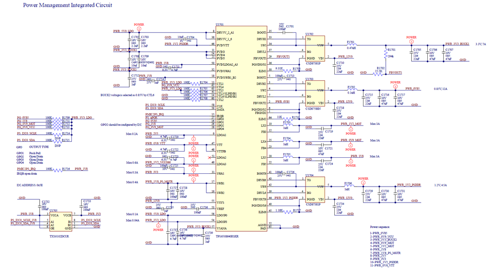
  • This is my schematic design

  • I used the resistor values in my board as follows:

    RILIM for BUCK1: 13K 

    RILIM for BUCK2: 27K

    RILIM for BUCK6:  10K

  • Hi Ömer,

    There are a couple things to point out here:

    • For the TPS6508640, you need to remove the resistor divider on FBVOUT1. BUCK1 feedback pin is looking for 3.3V and the resistor divider will cause incorrect regulation in this situation.
    • According to the TPS6508640 power up sequence shown in the datasheet, BUCK2 should power up once CTL3 is pulled high.

    Can you share some scope captures showing the power up sequence in order? Start with VSYS, LDO3P3, LDP5P0, and CTL3 in one scope capture and move through the sequence (show the rising edge of each signal with the time scale and voltage scale indicated clearly).

    You can read registers 0xB2 through 0xB6 to check for a power fault flag. Look for bits that are latched to a value of 1b. You can also check register 0x02 for more information about the shutdown source if the IC is resetting. See Section 8.13 in the datasheet for register bit field descriptions.

    Regards,

    James

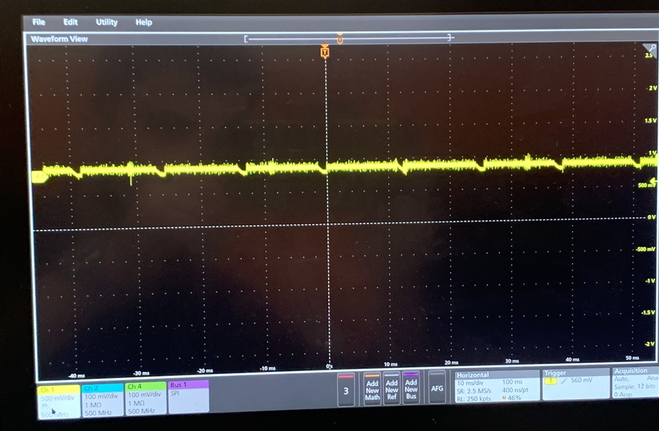
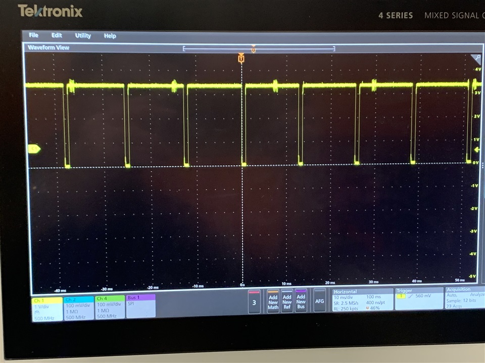
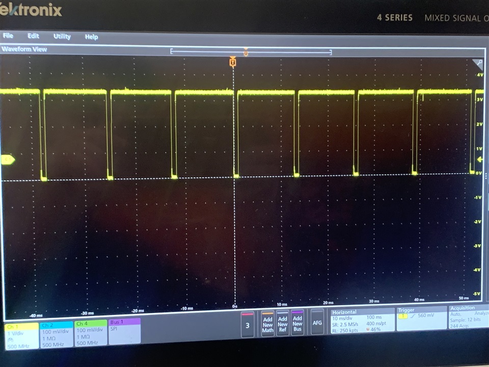
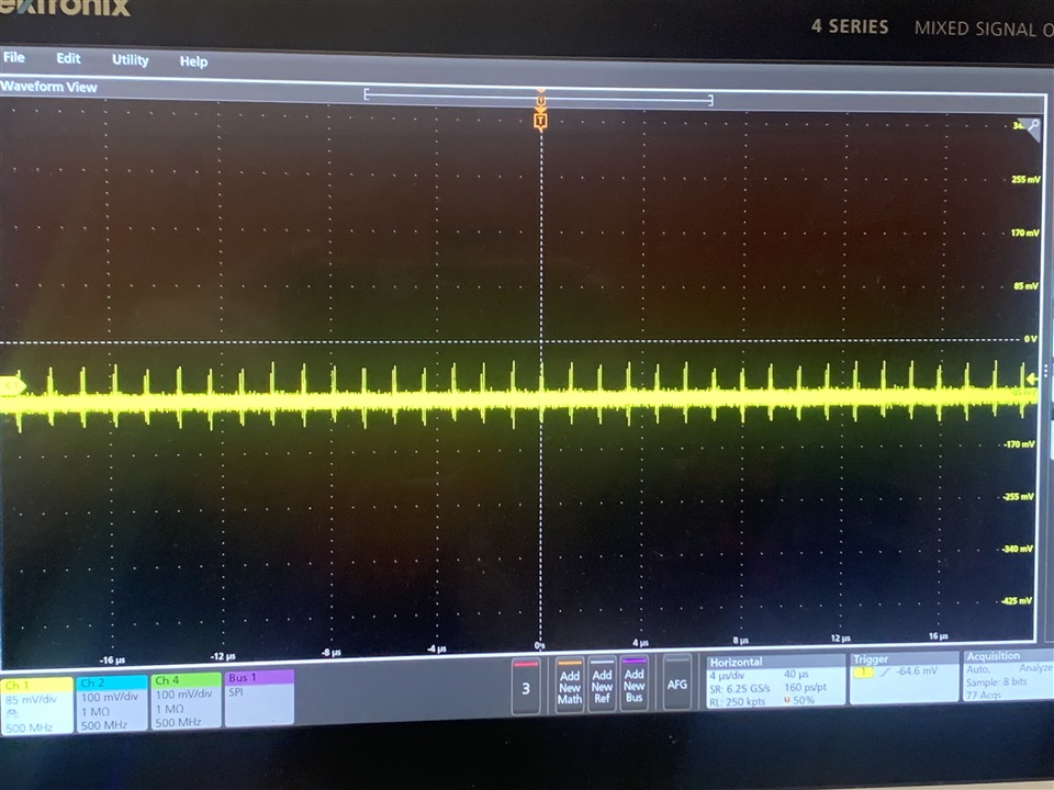
  • The issue I mentioned before was caused by a soldering problem. Currently, BUCK2 (0.85V) opened with a periodic wave. BUCK2_PG (PG_0V85V) also opened with a periodic wave. Therefore, a periodic wave came to CTL4 (PG_0V9_VCU). Finally, BUCK1 (3.3V) did not turn on. I am sharing the oscilloscope images of each below:

  • This is BUCK2 waveform:

    this is GPO1(BUCK2_PG) waveform:


    This is  CTL4(PG_0V9_VCU) waveform:


    this is BUCK1 waveform:

  • LDO5, LDO3P3 and CTL3 are stable as they should be.

  • For the TPS6508640, you need to remove the resistor divider on FBVOUT1. BUCK1 feedback pin is looking for 3.3V and the resistor divider will cause incorrect regulation in this situation.

    Thanks for pointing it out. I removed the resistor divider on FBVOUT1. I connected this pin directly with PWR_3V3_BUCK1.

  • Hi Ömer,

    This waveform behavior indicates that the PMIC is repeatedly resetting due to a power fault. Can you read registers 0xB2 through 0xB6 to see which power rail is reporting a fault.

    Regards,

    James