- Ask a related questionWhat is a related question?A related question is a question created from another question. When the related question is created, it will be automatically linked to the original question.
Questions relate to information given about the LMG3410R070 requirements relating to the ground planes and source connection regarding termination of bypass capacitors and the boost inductor. From data sheet - SNOSD10F –APRIL 2016–REVISED MAY 2020
Terms used are "Signal ground", ground, SOURCE plane and SOURCE pin.
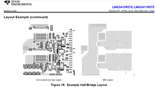
Their use is not clear in the data sheet as it appears there are conflicts with the lay-out example shown in the data sheet. Figure 19.
“ 11.1.2 Signal Ground Connection (page 24)
The LMG341xR070's SOURCE pin is also signal ground reference. The signal GND plane should be connected to SOURCE with low impedance kelvin connection. In addition, the return path for the passives associated to the driver (e.g. bypass capacitance) must be connected to the GND plane. In Figure 19, local signal GND planes are located on the second copper layer to act as the return for the local circuitry. The local signal GND planes are isolated from the high-current SOURCE plane except the kelvin connection at the source pin through enough low impedance vias.”
Question 1
Please clarify, is "signal GND plane" the same as "GND plane". In the lay-out example given in the data sheet there is confusion as C8 -Figure 14 Schematic Page 17 and C8 -Figure 19 Example Half-Bridge Layout appears to be connected to "signal GND plane by two vias and directly to Q1 (Top GaN) Source. This appears to conflict with Kelvin connection as the "signal GND" is connected to "Q1- source in two places.
Other Clauses using these terms
11.1.3 Bypass Capacitors (page 24) - what does ground plane refer to in this instance.
9.2.2.3 Buck-Boost Converter Design ( page 19) - Data sheet says "... This inductor is connected between the BBSW pin and ground. A 2.2 μF, 25V 0805 bypass capacitor is required between VNEG and ground. ..."
Question 2
2.2u capacitor is connected to Source ground. Inductor is connected to the signal GND in Figure 19 Example Half-Bridge Layout? – Why, would this not inject peak currents into signal ground?
Could you please clarify the terminology used in the data sheet.
Terms used are "Signal ground", ground, SOURCE plane and SOURCE pin.
Thanks,
Ed