


Other Parts Discussed in Thread: LM2577, TPS54040,
Dear TI team.
Switcher IC datasheets usually don't provide much information about the accuracy and stability of its internal error amplifier and voltage reference. The manufacturer assumes that its accuracy is adequate for general-purpose applications. However, applications like photomultiplier tube biasing require a much higher degree of supply voltage stability over time and temperature.
One possible solution is to bypass the internal error amplifier of the switcher IC and use an external operational amplifier instead. The output of the external error amplifier is connected to the frequency correction pin of the switcher IC, thus closing the feedback loop. This approach is similar to the solution described in the appnote "Snva559 Switching regulators" chapter "Increasing Available Load Power in an LM2577 Boost Regulator."
Some prototyping has been done on TPS54040 and TPS61170 as switched current sources for resonant Royer converters, and it has yielded positive results. The circuit design should be self-explanatory, and I hope that I have managed to draw it clearly. 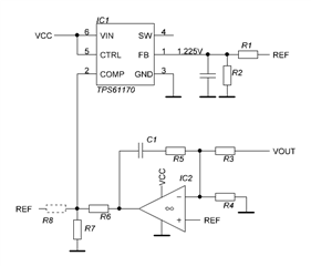
Here are the brief results of the testing. IC1 starts to switch when the voltage at the comp pin is above 500 mV and stops when it reaches 1 volt. Thus, the divider R6-R7 scales down the output voltage of the new error amplifier to prevent latch-up of the whole circuit. Voltage above 1 volt at the comp pin is treated by the internal circuitry as output overload. R8 can be added to pre-bias the comp pin. The original FB pin of IC1 is supplied with a voltage close to its internal reference to disable internal overload protection circuitry and minimize the original error amplifier output current. C1 and R5, together with R3, create a type 2 compensation network similar to the original one.
Before any significant scale production, I thought it would be a good idea to consult with the manufacturer. Can the TI team provide any advice or guidelines for this unconventional circuit application? I'm not constrained to a particular part number; any small to medium power switcher will work.
